Inside NVIDIA GPUs: Anatomy of high performance matmul kernels
From GPU architecture and PTX/SASS to warp-tiling and deep asynchronous tensor core pipelines
September 29, 2025
In this post, I will gradually introduce all of the core hardware concepts and programming techniques that underpin state-of-the-art (SOTA) NVIDIA GPU matrix-multiplication (matmul) kernels.
Why matmul? Transformers spend most of their FLOPs inside matmuls (linear layers in MLP, attention QKV projections, output projections, etc.) both during training and inference. These operations are embarrassingly parallel, making them a natural fit for GPUs. Finally, understanding how matmul kernels work gives you the toolkit to design nearly any other high-performance GPU kernel.
This post is structured into four parts:
- Fundamentals of NVIDIA GPU architecture: global memory, shared memory, L1/L2 cache, impact of power throttling on SOL, etc.
- GPU assembly languages: SASS and PTX
- Designing near-SOTA synchronous matmul kernel: the warp-tiling method
- Designing SOTA asynchronous matmul kernels on Hopper: leveraging tensor cores, TMA, overlapping computation with loads/stores, Hilbert curves, etc.
My aim is for this post to be self-contained: detailed enough to stand on its own, yet concise enough to avoid becoming a textbook.
This is the first part of a broader series. In the following posts, I (aspirationally) plan to cover:
- Designing SOTA matmul kernels on Blackwell GPUs
- Exploring GPU architecture through microbenchmarking experiments
- Designing SOTA multi-GPU kernels
- Demistifying memory consistency models (the GPU equivalent of the tokenizer: the critical component that quietly makes the system run, but still puzzles most devs)
Fundamentals of NVIDIA GPU architecture
To write performant GPU kernels, you need a solid mental model of the hardware. This will become clear very quickly as we dive into hardware architecture.
In this post, I focus on the Hopper H100 GPU. If you understand Hopper at a deep level, adapting your knowledge to future architectures (Blackwell, Rubin) or earlier ones (Ampere, Volta) becomes straightforward.
At the highest level, a GPU performs two essential tasks:
- Move and store data (the memory system)
- Do useful work with the data (the compute pipelines)
The block diagram of H100 below reflects this division: components in blue represent memory or data movement, while components in red are compute (hot) units.
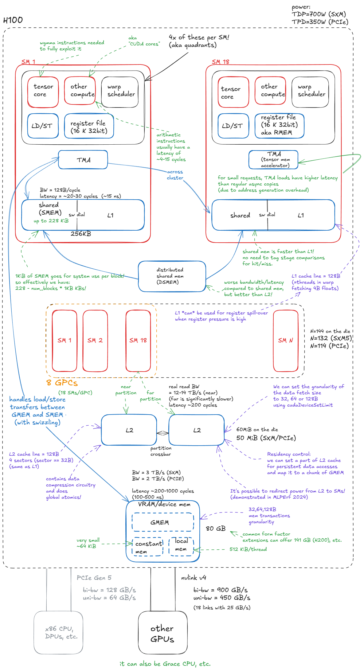
Memory
The memory system in a GPU is highly hierarchical, much like in CPU architectures.
This hierarchy is dictated by physics and circuit design: SRAM cells are faster but larger (the control circuitry that enables their speed also increases their area), while DRAM cells are smaller / denser but slower. The result is that fast memory is lower capacity and expensive, while slower memory can be provided in much larger quantities. We will cover DRAM cell/memory in more detail later.
This trade-off between capacity and latency is exactly why cache hierarchies exist. In an ideal world, every compute unit would sit next to a vast pool of ultra-fast memory. Since that is physically impossible, GPU designers compromise: a small amount of fast memory is placed close to compute, backed by progressively larger pools of slower memory further away. This organization maximizes overall system throughput.
The GPU memory system consists of:
- Device memory (VRAM). In CUDA terminology, "device" memory refers to off-chip DRAM—physically separate from the GPU die but packaged together on the same board—implemented as stacked HBM. It hosts global memory (GMEM), per-thread "local" memory (register spill space), etc.
- L2 cache. A large, k-way set-associative cache built from SRAM. It is physically partitioned into two parts; each SM connects directly to only one partition and indirectly to the other through the crossbar.
- Distributed shared memory (DSMEM). The pooled shared memories (SMEM) of a physically close group of SMs (a GPC).
- L1 cache and Shared memory
- L1 cache. A smaller, k-way set-associative SRAM cache private to each SM.
- Shared memory (SMEM). Programmer-managed on-chip memory. SMEM and L1 share the same physical storage, and their relative split can be configured in software.
- Register file (RMEM). The fastest storage, located next to the compute units. Registers are private to individual threads. Compared to CPUs, GPUs contain far more registers, and the total RMEM capacity is of the same size as the combined L1/SMEM storage.
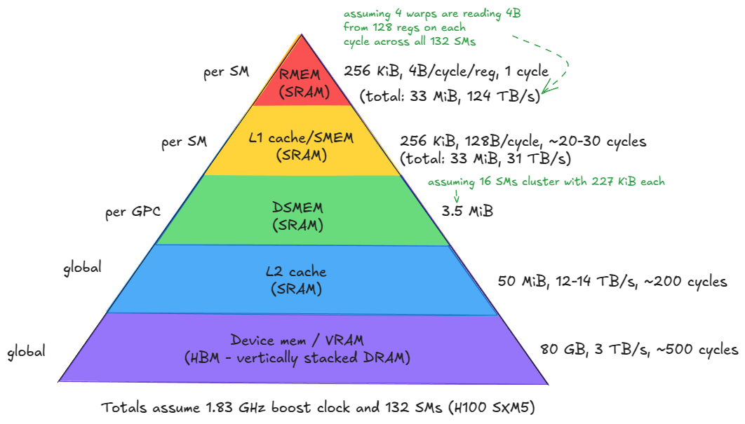
Moving from device memory down to registers (levels 1-5), you see a clear trend: bandwidth increases by orders of magnitude, while both latency and capacity decrease by similar orders of magnitude.
A few immediate implications follow:
- Keep the most frequently accessed data as close as possible to the compute units.
- Minimize accesses to the lower levels of the hierarchy, especially device memory (GMEM).
One additional component worth noting is the Tensor Memory Accelerator (TMA), introduced with Hopper. TMA enables asynchronous data transfers between global memory and shared memory, as well as across shared memories within a cluster. It also supports swizzling to reduce bank conflicts—we'll cover these details just in time (pun intended).
Compute
Switching from memory to compute, the fundamental unit is the streaming multiprocessor (SM). Hopper H100 (SXM5) integrates 132 SMs in total.
SMs are grouped into graphics processing clusters (GPCs): each GPC contains 18 SMs, and there are 8 GPCs on the GPU. Four GPCs connect directly to one L2 partition, and the other four to the second partition.
The GPC is also the hardware unit that underpins the thread-block cluster abstraction in CUDA — we'll come back to the programming model shortly.
One point relevant to clusters: earlier I said each GPC has 18 SMs, so with 8 GPCs we'd expect 144 SMs. But SXM/PCIe form factors expose 132 or 114 SMs. Where's the discrepancy? It's because that 18 × 8 layout is true only for the full GH100 die — in actual products, some SMs are fused off. This has direct implications for how we choose cluster configurations when writing kernels. E.g. you can't use all SMs with clusters spanning more than 2 SMs.
Finally, note that “graphics” in graphics processing cluster (GPC) is a legacy term. In modern server-class GPUs, these clusters serve purely as compute/AI acceleration units rather than graphics engines. Same goes for GPUs, drop the G, they're AI accelerators.
Beyond the L1/SMEM/TMA/RMEM components already mentioned (all physically located within the SM), each SM also contains:
- Tensor Cores. Specialized units that execute matrix multiplications on small tiles (e.g.,
64x16 @ 16x256) at high throughput. Large matrix multiplications are decomposed into many such tile operations, so leveraging them effectively is critical for reaching peak performance. - CUDA cores and SFUs. The so-called "CUDA cores" (marketing speech) execute standard floating-point operations such as FMA (fused multiply-add:
c = a * b + c). Special Function Units (SFUs) handle transcendental functions such assin,cos,exp,log, but also algebraic functions such assqrt,rsqrt, etc. - Load/Store (LD/ST) units. Circuits that service load and store instructions, complementary to the TMA engine.
- Warp schedulers. Each SM contains schedulers that issue instructions for groups of 32 threads (called warps in CUDA). A warp scheduler can issue one warp instruction per cycle.
Each SM is physically divided into four quadrants, each housing a subset of the compute units described above.
That leads to the following insight:
An SM can issue instructions from at most four warps simultaneously (i.e., 128 threads in true parallel execution at a given cycle).
However, an SM can host up to 2048 concurrent threads (64 warps). These warps are resident and scheduled in and out over time, allowing the hardware to hide memory/pipeline latency.
In other words, instruction parallelism (how many threads start executing an instruction on a given cycle) is limited to 128 threads per SM at once (4 32-wide warp instructions), while concurrency (how many threads are tracked in the scheduler and eligible to run) extends to 2048 threads.
Speed of light and power throttling
Since we buy NVIDIA GPUs for compute, it is natural to ask: what is the ceiling—the maximum compute throughput of a GPU? This is often referred to as the "speed of light" (SoL) performance: the upper bound dictated by the physical characteristics of the chip.
There are multiple ceilings depending on the data type. In LLM training workloads, bfloat16 (bf16) has been the dominant format in recent years, though fp8 and 4-bit formats are becoming increasingly important (for inference fp8 is fairly standard).
The peak throughput is calculated as: perf = freq_clk_max * num_tc * flop_per_tc_per_clk
or in words: maximum clock frequency × number of tensor cores × FLOPs per tensor core per cycle.
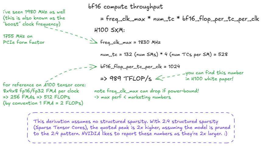
- FLOP = a single floating-point operation.
- FLOP/s = a unit of throughput: floating-point operations per second.
- FLOPs (with a lowercase s) = the plural of FLOP (operations).
- FLOPS (all caps) is often misused to mean throughput, but strictly speaking should only be read as "FLOPs" (the plural of FLOP). FLOPS used as FLOP/s is SLOP! :)
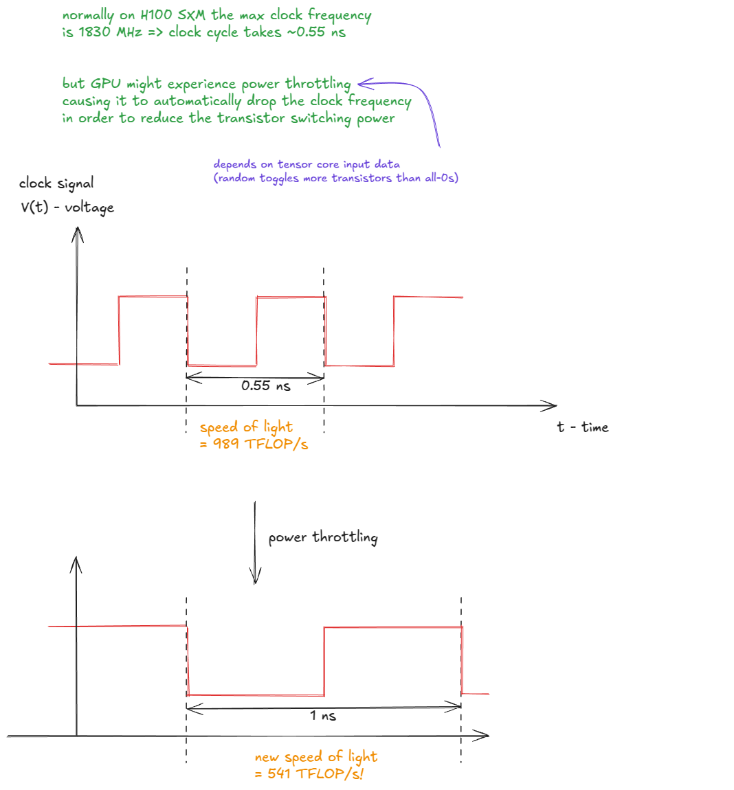
I left one hint in the figure above: the "speed of light" is not actually constant (I guess this is where the analogy breaks down).
In practice, the peak throughput depends on the actual clock frequency, which can vary under power or thermal throttling. If the GPU clock drops, so does the effective speed of light:
That's as much hardware detail as we need for the moment.
Next, we'll shift our focus to the CUDA programming model, before diving one level deeper into the hardware and eventually ascending toward CUDA C++ land.
CUDA programming model
The CUDA programming model naturally maps onto the GPU hardware and memory hierarchy.
The key abstractions are:- thread
- warp (32 threads)
- thread block
- thread block cluster
- grid (of thread blocks or clusters)
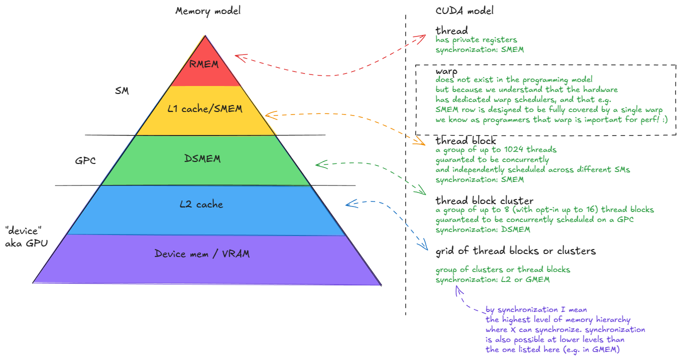
Every thread is "aware" of its position in the CUDA hierarchy through variables such as gridDim, blockIdx, blockDim, and threadIdx. Internally, these are stored in special registers and initialized by the CUDA runtime when a kernel launches.
This positional information makes it easy to divide work across the GPU. For example, suppose we want to process a 1024×1024 image. We could partition it into 32×32 thread blocks, with each block containing a 32×32 arrangement of threads.
Each thread can then compute its global coordinates, e.g.
const int x = blockIdx.x * blockDim.x + threadIdx.x
const int y = blockIdx.y * blockDim.y + threadIdx.y
and use those to fetch its assigned pixel from global memory (image[x][y]), perform some pointwise operation, and store the result back.
Here is how those variables relate to each other:
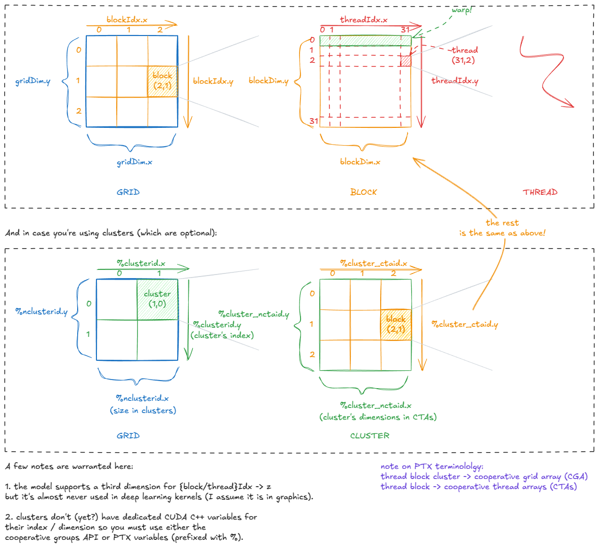
As noted in the image, in practice we mostly use 1D or 2D grid/cluster/block shapes. Internally, though, they can always be reorganized logically as needed.
threadIdx.x runs from 0-1023 (a 1D block of 1024 threads) we can split it into x = threadIdx.x % 32 and y = threadIdx.x / 32, effectively reshaping the block into a 32×32 logical 2D layout.Connecting the CUDA model back to the hardware, one fact should now be clear: a thread block should contain at least 4 warps (i.e., 128 threads).
Why?
- A thread block is resident on a single SM.
- Each SM has 4 warp schedulers—so to fully utilize the hardware, you don't want them sitting idle.
We'll dive deeper into this later, but note that on Hopper the warp-group (4 warps) is the unit of execution for WGMMA (matmul) tensor core instructions.
Also, with persistent kernels, we often launch just one thread block per SM, so it's important to structure work so that all warp schedulers are kept busy.
Armed with the CUDA programming model terminology, we can now continue our descent into the GPU's architecture.
GMEM Model
Let's dive into GMEM. As noted earlier, it is implemented as a stack of DRAM layers with a logic layer at the bottom (HBM). But what exactly is DRAM?
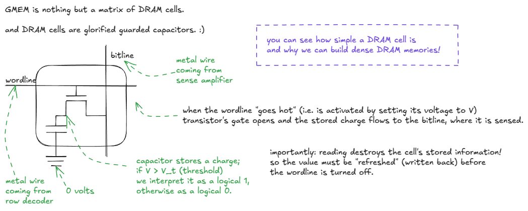
Now that we understand how a single bit is stored, let's zoom out to the entire memory matrix. At a high level, it looks like this:
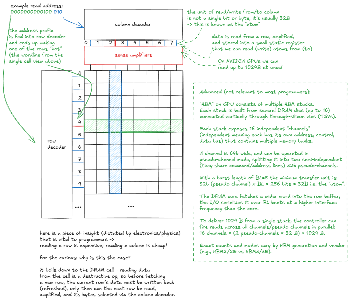
Thus we conclude: access patterns matter because of the physics of DRAM cells. Here is an example:
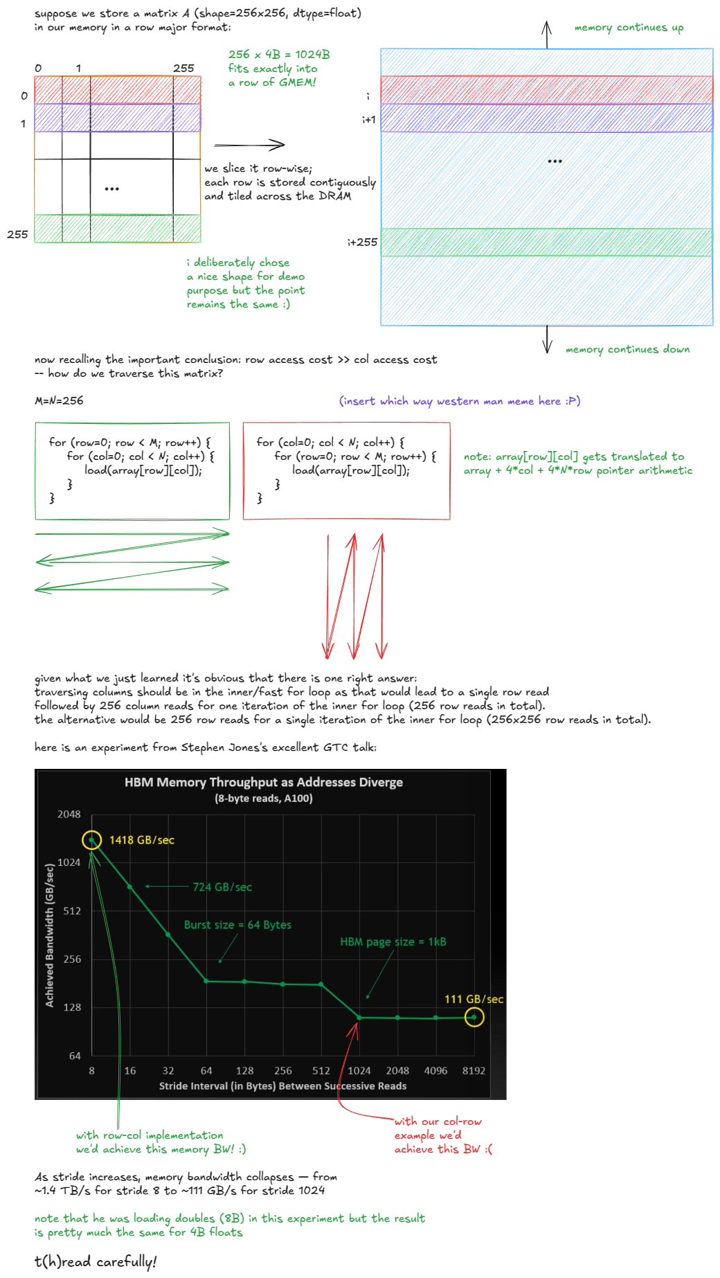
If the matrix in our example were column-major, the situation would flip: elements in a column would be stored contiguously, so the efficient choice would be to traverse rows in the inner loop to avoid the DRAM penalty.
So when people say “GMEM coalescing is very important”, this is what they mean: threads should access contiguous memory locations to minimize the number of DRAM rows touched.
Next, let's turn our attention to how SMEM works.
SMEM Model
Shared memory (SMEM) has very different properties from GMEM. It is built from SRAM cells rather than DRAM, which gives it fundamentally different speed and capacity trade-offs.
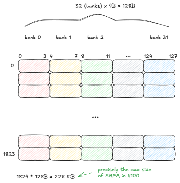
SMEM can serve data from all 32 banks (128B) in a single cycle — but only if one rule is respected:
Threads in a warp must not access different addresses within the same bank. Otherwise, those requests are serialized across multiple cycles.
This situation is known as a bank conflict. If N threads access different addresses of the same bank, the result is an N-way bank conflict and the warp’s memory request takes N cycles to complete.
In the worst case, all 32 threads target different addresses in the same bank, and throughput drops by a factor of 32.
To illustrate, suppose the warp size were 5. The two access patterns below would take 3 cycles and 1 cycle to serve, respectively:
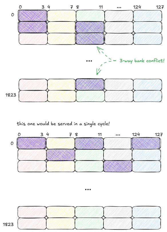
Importantly: if multiple threads in a warp access the same address within a bank, SMEM can broadcast (or multicast) that value to all of them.
In the below example, the request is served in a single cycle:
- Bank 1 can multicast a value to 2 threads.
- Bank 2 can multicast a value to 3 threads.
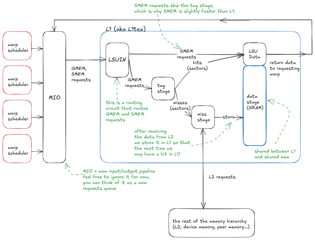
L1 Model
We've already seen that L1 and SMEM share the same physical storage, but L1 adds a hardware-managed scaffolding layer around that storage.
At a high level, the logic flow of the L1 cache is:
- A warp issues a memory request (either to SMEM or GMEM).
- Requests enter the MIO pipeline and are dispatched to the LSUIN router.
- The router directs the request: SMEM accesses are served immediately from the data array, while GMEM accesses move on to the tag-comparison stage.
- In the tag stage, the GMEM address tags are compared against those stored in the target set to determine if the data is resident in L1.
- On a hit, the request is served directly from the data array (just like SMEM).
- On a miss, the request propagates to L2 (and beyond, if necessary, up to GMEM or peer GPU memory). When the data returns, it is cached in L1, evicting an existing line, and in parallel sent back to the requesting warp.
Here is the system I just described:
Let's go one level deeper and look at the tag stage and data stage in detail:
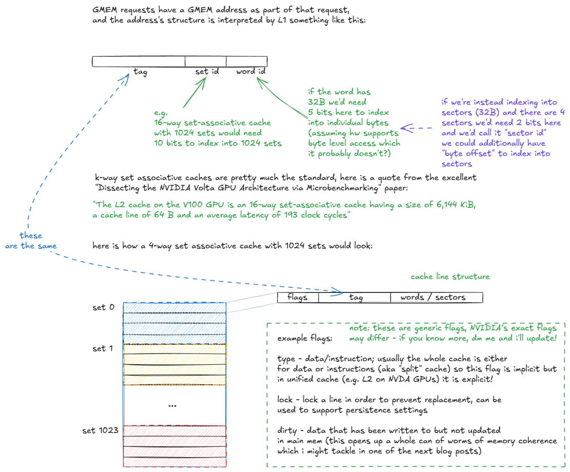
When a GMEM address enters the tag stage, the hit/miss logic unfolds as follows:
- The tag stage receives the GMEM address.
- The set id bits are extracted, and all cache lines (tags) in that set are checked.
- If a tag match is found (potential cache hit):
- The line's validity flags are examined.
- If invalid → it is treated as a cache miss (continue to step 4).
- If valid → the requested sectors are fetched from the data array and delivered to the warp's registers.
- The line's validity flags are examined.
- If no match is found (cache miss), the request is routed to the rest of the memory hierarchy (L2 and beyond).
- When the data returns from L2, it is stored in the set, evicting an existing line according to the replacement policy (e.g., pseudo-LRU), and in parallel delivered to the requesting warp.
Note that L2 is not too dissimilar from L1, except that it is global (vs. per-SM), much larger (with higher associativity), partitioned into two slices connected by a crossbar, and supports more nuanced persistence and caching policies.
With this, we've covered the key GPU hardware components needed to understand the upcoming sections.
I mentioned earlier that understanding Hopper is an excellent foundation for both future and past generations of NVIDIA GPUs.
The biggest generational jump so far was from Ampere → Hopper, with the introduction of:
- Distributed Shared Memory (DSMEM): direct SM-to-SM communication for loads, stores, and atomics across the SMEMs of an entire GPC.
- TMA: hardware unit for asynchronous tensor data movement (GMEM ↔ SMEM, SMEM ↔ SMEM).
- Thread Block Clusters: a new CUDA programming model abstraction for grouping blocks across SMs.
- Asynchronous transaction barriers: split barriers that count transactions (bytes) instead of just threads.
Ampere (e.g. A100) itself introduced several key features:
- tf32 and bf16 support in Tensor Cores.
- Asynchronous copy (GMEM → SMEM) with two modes: bypass L1 and access L1.
- Asynchronous barriers (hardware-accelerated in shared memory).
- CUDA task graphs, which underpin CUDA graphs in PyTorch and reduce CPU launch + grid initialization overhead.
- Warp-level reduction instructions exposed through CUDA Cooperative Groups (enabling warp-wide, integer dtype, reductions in a single step, without shuffle patterns).
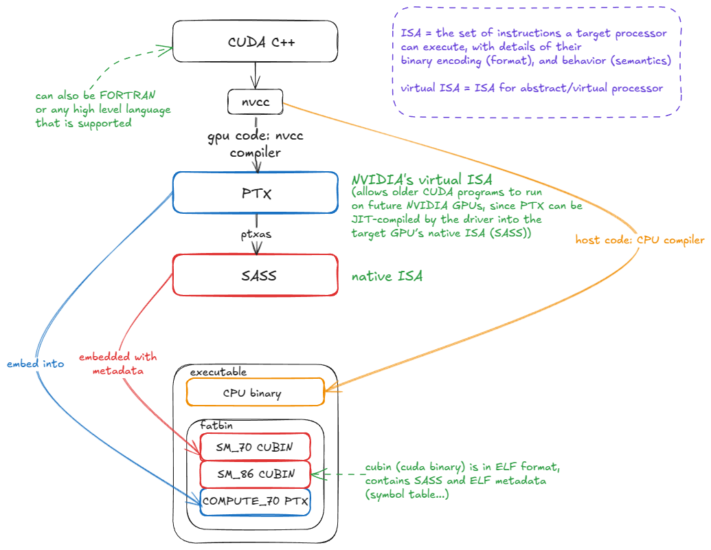
GPU assembly languages: PTX and SASS
Let's move one level above the hardware to its ISA (Instruction Set Architecture). An ISA is simply the set of instructions a processor (e.g., an NVIDIA GPU) can execute, along with their binary encodings (opcodes, operands, etc.) and behavioral semantics. Together, these define how programmers can direct the hardware to do useful work.
The human-readable form of an ISA is known as the assembly: instead of writing raw binary like 0x1fff…3B, a programmer uses mnemonics such as FMA R12, R13, R14, R15 to express the same instruction.
On NVIDIA GPUs, the native ISA is called SASS. Unfortunately, it is poorly documented—especially for the most recent GPU generations. Some older generations have been partially or fully reverse engineered, but official documentation remains limited. You can find the documentation here [6].
PTX is NVIDIA's virtual ISA: an instruction set for an abstract GPU. PTX code is not executed directly; instead, it is compiled by ptxas into the native ISA (SASS).
The key advantage of PTX is forward compatibility. A CUDA program compiled to PTX a decade ago can still run on a modern GPU like Blackwell. It may not exploit the latest hardware features efficiently, but it will execute correctly.
This works because PTX is embedded into the CUDA binary alongside native SASS. When the binary runs on a future GPU, if matching SASS code is not already present, the PTX is JIT-compiled into SASS for the target architecture:
Why care about PTX/SASS?
Because this is where the last few percent of performance can be found. On today's scale, those "few percent" are massive: if you're training an LLM across 30,000 H100s, improving a core kernel's performance by even 1% translates into millions of dollars saved.
As my friend Aroun likes to put it: when writing large scale training/inference kernels, we care about O(NR), not O(N). (Here, NR = nuclear reactors.) In other words, there are likely no new asymptotic complexity classes waiting to be discovered — the big wins are (mostly) gone. But squeezing out ~1% efficiency across millions of GPUs is the equivalent of saving a few SMRs (small modular reactors) worth of energy.
It's not that understanding SASS means you'll start writing CUDA kernels directly in SASS. Rather, when writing CUDA C++ you want to stay tightly coupled to the compiler's output (PTX/SASS). This lets you double-check that your hints (e.g., #pragma unroll to unroll a loop, or vectorized loads) are actually being lowered into the expected instructions (e.g., LDG.128).
A great example of the performance hidden in these low-level details comes from the now-famous Citadel paper, "Dissecting the NVIDIA Volta GPU Architecture via Microbenchmarking" [8]. The authors tweaked SASS to avoid memory bank conflicts and boosted performance from 132 GFLOP/s to 152 GFLOP/s — a 15.4% improvement.
Note also that some instructions have no equivalent in CUDA C++; you simply have to write inline PTX! We'll see examples of this later in Chapter 4.
Now that (hopefully) I've convinced you that PTX/SASS matters, let's introduce the simplest possible matmul kernel, which will serve as our running example for the rest of this chapter. After that we will analyze its assembly in great depth.
Let's begin with the simplest case: a naïve matrix-multiplication kernel for a "serial processor" like the CPU:
for (int m = 0; m < M; m++) {
    for (int n = 0; n < N; n++) {
        float tmp = 0.0f;  // accumulator for dot product
        for (int k = 0; k < K; k++) {
            tmp += A[m][k] * B[k][n];  // A and B are input matrices
        }
        C[m][n] = tmp;  // C is the output matrix
    }
}
We loop over the rows (m) and columns (n) of the output matrix (C), and at each location compute a dot product (C[m,n] = dot(a[m,k],b[k,n])). This is the textbook definition of matmul:
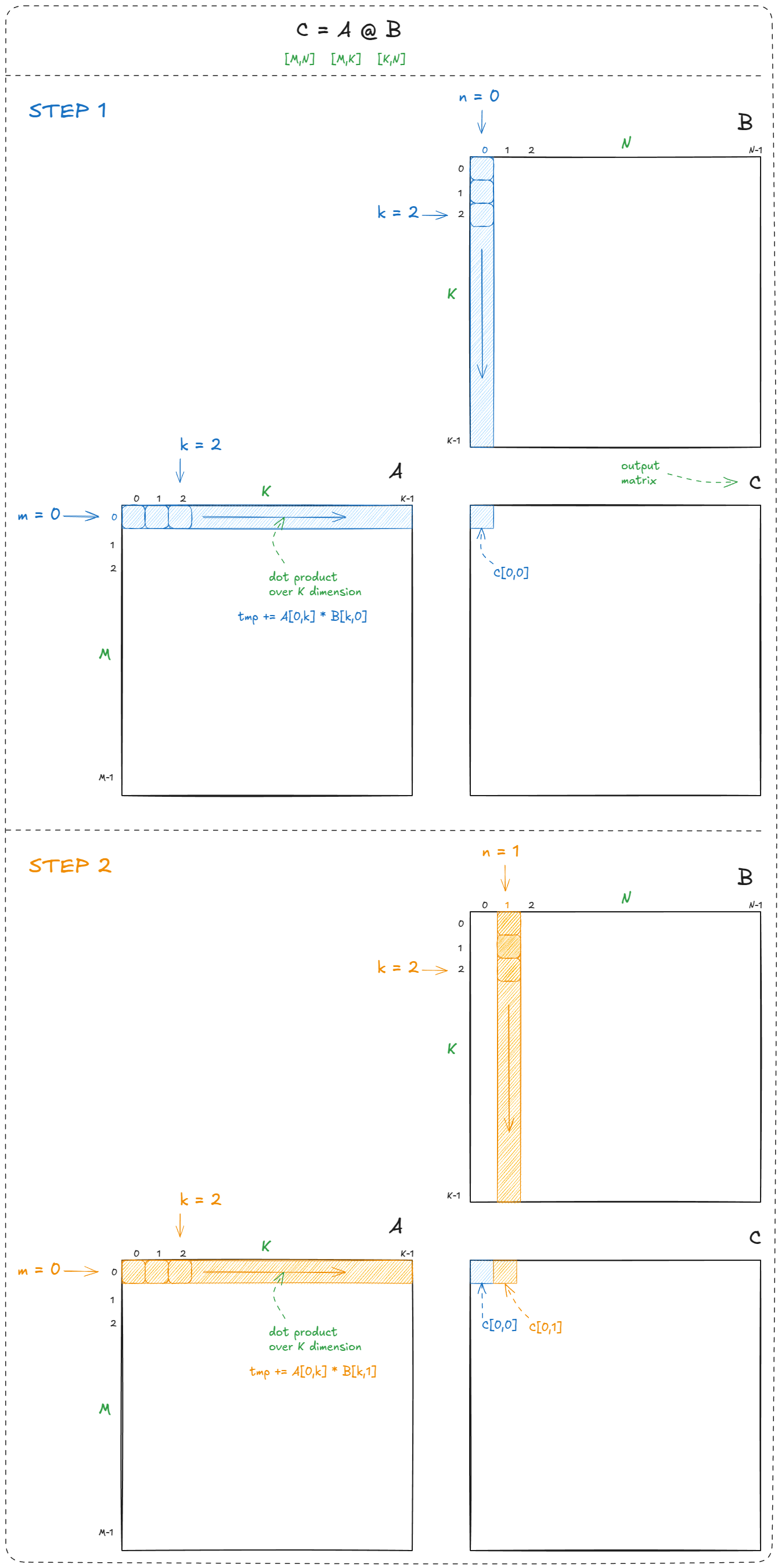
In total, matrix multiplication requires M × N dot products. Each dot product performs K multiply-adds, so the total work is 2 × M × N × K FLOPs (factor of 2 because, by convention, we count FMA = multiply + add).
Where's the parallelism?
All of these dot products are independent. There's no reason why computing C[0,1] should wait for C[0,0]. This independence means we can parallelize across the two outer loops (over m and n).
With that insight, let's look at the simplest possible GPU kernel. We'll use a slightly more general form: C = alpha * A @ B + beta * C. This is the classic GEMM (General Matrix Multiply). Setting alpha = 1.0 and beta = 0.0 recovers the simpler C = A @ B.
Kernel code:
// __global__ keyword declares a GPU kernel
__global__ void naive_kernel(int M, int N, int K, float alpha,
                                          const float *A, const float *B,
                                          float beta, float *C) {
  int BLOCKSIZE=32;

  const int row = blockIdx.x * BLOCKSIZE + (threadIdx.x / BLOCKSIZE);
  const int col = blockIdx.y * BLOCKSIZE + (threadIdx.x % BLOCKSIZE);

  if (row < M && col < N) {  // guard in case some threads are outside the range
    float tmp = 0.0;
    // compute dot product
    for (int i = 0; i < K; ++i) {
      tmp += A[row * K + i] * B[i * N + col];
    }
    // GEMM: C = alpha * A @ B + beta * C
    C[row * N + col] = alpha * tmp + beta * C[row * N + col];
  }
}
And we launch it like this:
// create as many blocks as necessary to map all of C
dim3 gridDim(CEIL_DIV(M, 32), CEIL_DIV(N, 32), 1);
// 32 * 32 = 1024 thread per block
dim3 blockDim(32 * 32);
// launch the asynchronous execution of the kernel on the device
// the function call returns immediately on the host
naive_kernel<<<gridDim, blockDim>>>(M, N, K, alpha, A, B, beta, C);
You can observe a few things here:
- Kernels are written from the perspective of a single thread. This follows the SIMT (Single Instruction, Multiple Threads) model: the programmer writes one thread's work, while CUDA handles the launch and initialization of grids, clusters, and blocks. (Other programming models, such as OpenAI's Triton [22], let you write from the perspective of a tile instead.)
- Each thread uses its block and thread indices (the variables we discussed earlier) to compute its (
row,col) coordinates inCand write out the corresponding dot product. - We tile the output matrix using as many 32×32 thread blocks (1024 threads) as possible.
- If
MorNare not divisible by 32, some threads fall outside the valid output region ofC. That's why we include a guard in the code.
The last two points combined lead to a phenomenon commonly known as the tile quantization:
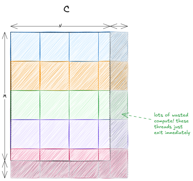
This effect is especially pronounced when the tiles are large relative to the output matrix. In our case, there's no issue since 32 divides 4096 exactly. But if the matrix size was, say, 33×33, then roughly 75% of the threads would end up doing no useful work.
The code could have been written more simply by passing a 2D block instead of a 1D one. In that case, we wouldn't need to hardcode the block size of 32 and we could use threadIdx.x and threadIdx.y. Internally, a 1D structure is effectively converted into 2D using index arithmetic:threadIdx.x / BLOCKSIZE and threadIdx.x % BLOCKSIZE so in practice it doesn't make much difference.
I originally adapted this code from Simon's blog [9] and focused on doing an in-depth PTX/SASS analysis on it (coming up soon), so I didn't want to repeat the hard work as slight code changes would lead to different PTX/SASS.
Let's take a closer look at what this kernel actually does. For the rest of this post, we'll assume M = N = 4096. All matrices in this example are in row-major format (in some later examples B will be column-major - standard convention).
The logical organization of threads looks like this:
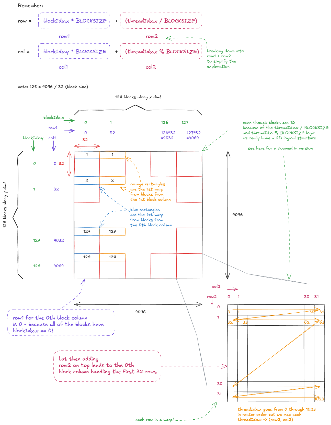
And the matmul logic itself looks like this:
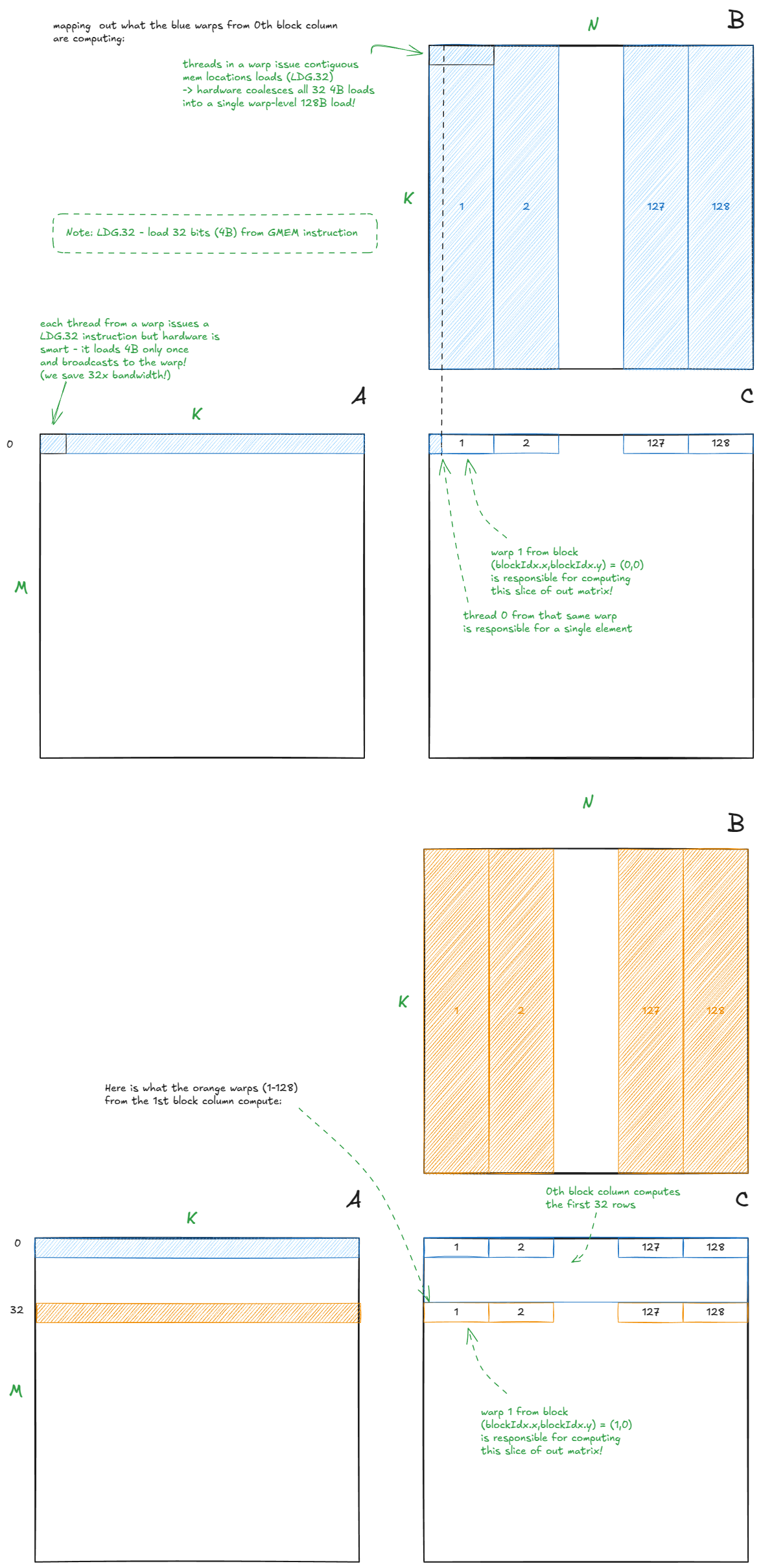
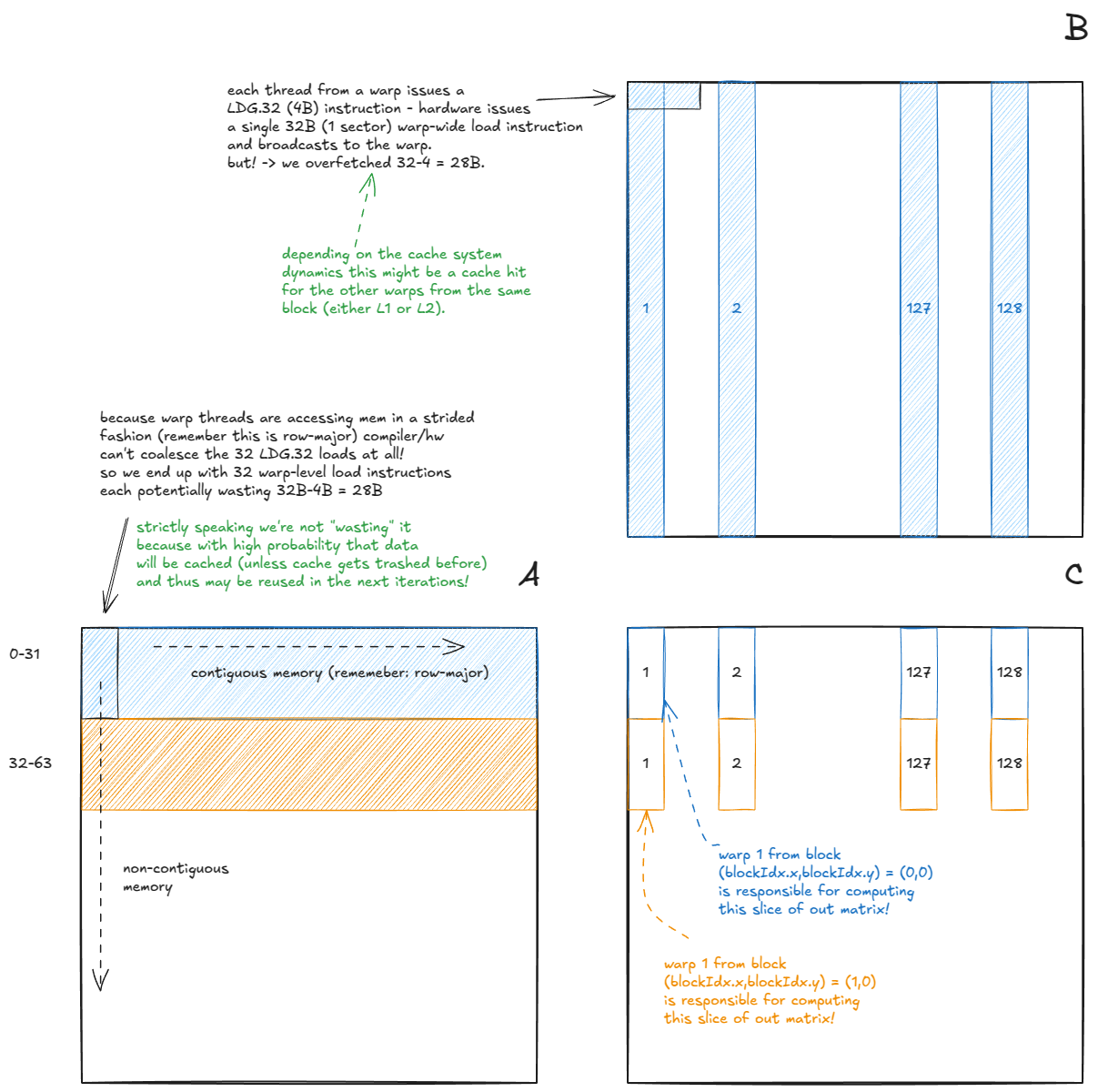
A few interesting optimizations happen automatically in hardware when our GMEM accesses are coalesced:
- (Matrix A) For a warp reading from
A, 32 per-threadLDG.32instructions (all from the same address) are merged into a single warp-levelLDG.32, whose result is broadcast to all threads in the warp. - (Matrix B) For a warp reading from
B, 32 consecutive per-threadLDG.32instructions are combined into a single 128B warp-level load. This relies on the threads reading along the contiguous dimension. If instead they read down a column (non-contiguous), the hardware would need to issue multiple warp-level instructions.
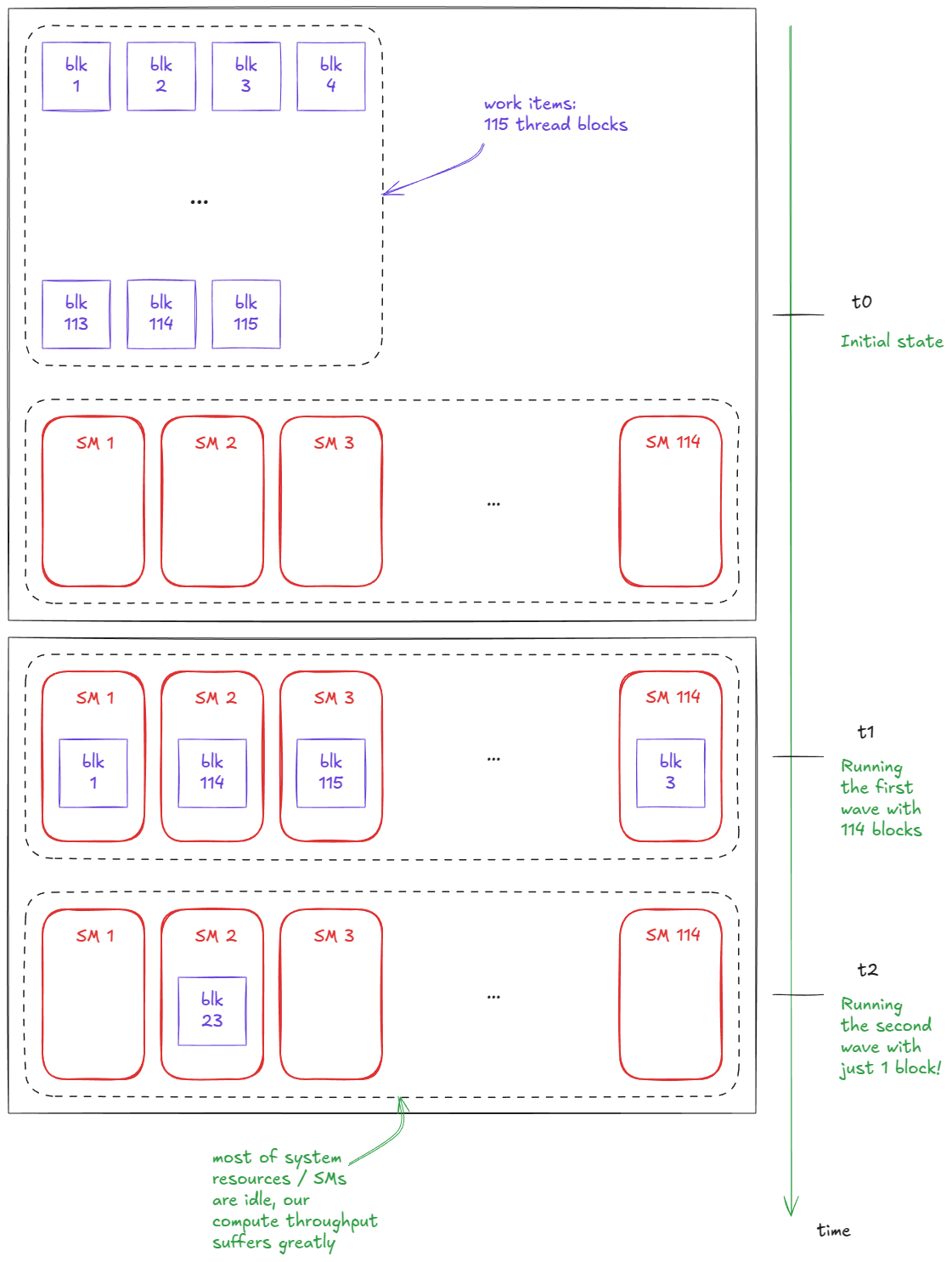
Notice that we launch (4096/32) * (4096/32) = 16,384 thread blocks in total. However, the H100 PCIe (the card I'm using) only has 114 SMs.
That raises the question: how many blocks can run concurrently on each SM?
In general, three resources limit concurrency:
- Registers
- Shared memory (SMEM)
- Threads/warps
From Nsight Compute profiler (ncu --set full -o out.ncu-rep naive_kernel, also see the next figure), we see that the kernel uses 32 registers per thread. With 1024 threads per block, that's 1024×32=32,768 registers per block. Since each SM has 65,536 registers (you can find these constants in CUDA C programming guide [10]) this caps us at 2 blocks per SM.
Tip. You can also pass --ptxas-options=-v when compiling to have the compiler report register usage and other resource counts. nvdisasm is helpful little tool as well.
On Hopper (compute capability 9.0), the maximum number of threads per SM is 2048. With 1024 threads per block, that again caps us at 2 blocks per SM.
Recall from the hardware chapter that, even if a kernel doesn't explicitly use SMEM, there's always a system-level overhead of 1024B per block. With the default SMEM allocation of 8192B per SM (without turning the dial up to 228 KiB), that would allow up to 8 blocks.
Putting it all together: max blocks/SM = min(2,2,8) = 2.
So, at any given time, this kernel can have up to 114×2 = 228 thread blocks resident on the GPU.
This means we'll need 16,384 / 228 = ~71.86 so-called waves in order to complete the matmul operation.
In CUDA terminology, occupancy usually refers to the number of concurrent blocks that can run on an SM. There's also a closely related definition:
Occupancy (warps): the ratio of active warps to the maximum number of warps per SM.
Here, "active warps" means the warps of a thread block after they've been allocated resources (registers, SMEM, etc.) at launch.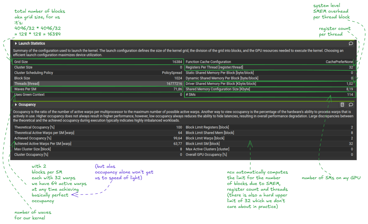
Worth mentioning here: just like tile quantization, there's also a concept of wave quantization. This effect is especially noticeable when the number of waves is small.
For example, suppose I launch a kernel with 114 blocks (exactly the number of SMs on my H100 PCIe). And suppose we can only run 1 block / SM at the time. With only one block per SM, the kernel finishes in a single wave. Now imagine I increase the launch to 115 blocks. Suddenly, execution time nearly doubles — because we need two waves — yet most of the resources in that second wave sit idle, with only a single block running:
With this basic analysis of the naive matmul kernel in place, let's now turn to the PTX/SASS view. Here are the compilation settings I used (Godbolt):
compilation settings:
nvcc 12.5.1

-O3  # the most aggressive standard-compliant optimization level, add loop unrolling, etc.
-DNDEBUG  # turn assert() into noop, doesn't matter for our simple kernel
--generate-code=arch=compute_90,code=[compute_90,sm_90a]  # embed PTX/SASS for H100
--ptxas-options=-v  # makes ptxas print per-kernel resource usage during compilation
-std=c++17  # compile the code according to the ISO C++17 standard, doesn't matter
# --fast-math  # not using, less important for this kernel
--use_fast_math. It trades numerical accuracy for speed and primarily affects fp32 ops. E.g., it replaces standard math functions with fast, approximate instrinsics (e.g. sinf -> __sinf), enables flush-to-zero (ftz) for denormals (very small floats below the minimum “normal” representable magnitude), etc.Below is the annotated PTX for the CUDA C++ kernel shown above. I decoded it manually to better internalize the ISA. Feel free to zoom in and take a moment to digest the structure (alternatively jump right after the figure to read my summary and then get back to the figure):
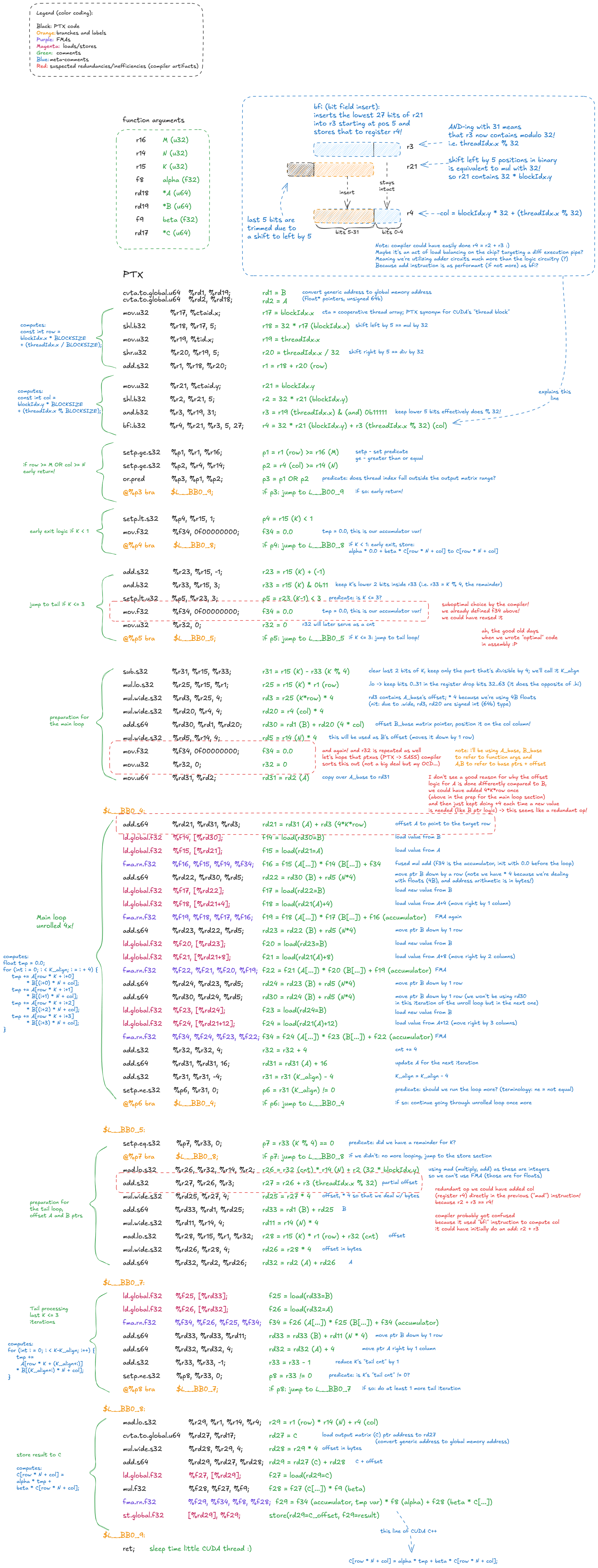
To summarize, here is the high-level flow of the PTX code:
- Compute the
rowandcolvariables. Interestingly, the compiler uses abfi(bit field insert) instruction to computecolinstead of a simple add of registersr2andr3. This may be an attempt to balance execution pipelines by routing work to a less-utilized unit — but note thatbfiitself is not inherently faster than add instruction. - Early exit if this thread is outside the valid range of
C(guard logic). - If
K < 1jump directly to storing toC(tmpwill be 0.0). - If
K <= 3jump to tail loop. - Otherwise, if
K > 3: compute the base offsets forAandBbefore entering the main loop. - Main loop (unrolled ×4). Perform 4 FMA steps per iteration, interleaved with loads and address arithmetic.
- Tail loop (
<= 3iterations). Execute the remaining dot-product steps without unrolling. - Epilogue: load the output value of
C, apply the GEMM update (alpha * A @ B + beta * C), and write the result back to global memory withst.global.f32.
A few compiler optimizations are visible here: early exits, loop unrolling, splitting into main and tail loops, and what looks like pipeline load-balancing (assuming my bfi hypothesis is correct).
The unrolling in particular is important because it exposes ILP. The warp doesn't need to be swapped out for another warp as quickly, since it still has independent instructions to issue — that's what helps hide latency.
What is ILP (Instruction-Level Parallelism)?
Instruction-Level Parallelism (ILP) is the amount of work a single warp can keep "in flight" at once by issuing independent instructions back-to-back. High ILP lets the warp scheduler issue a new instruction every cycle while earlier ones are still waiting out their latency.
Consider these 2 instruction streams (assume FMA takes 4 cycles):
1) Low ILP (fully dependent chain)
y = a * b + 1.0;     // uses a,b
z = y * c + 1.0;     // depends on y
w = z * c + 1.0;     // depends on z
Each FMA depends on the previous result => can not be scheduled in parallel => total latency = 12 (3*4) cycles.
2) High ILP (independent ops)
c0 = a0 * b0 + 1.0;
c1 = a1 * b1 + 1.0;
c2 = a2 * b2 + 1.0;
Three independent FMAs => the scheduler can issue them in consecutive cycles. Issue at cycles 0,1,2 results ready at 4,5,6 => total latency = 6 cycles.
That's why loop unrolling/ILP matters.
For debugging, you might want to disable loop unrolling to make PTX/SASS analysis easier. Just add: #pragma unroll 1.
Unrolling also reduces the number of branch (bra) instructions making the program more concise/efficient.
I did also observe a few compiler inefficiencies, such as:
- Unnecessary initialization of variables to 0.
- Overly complex computation of
A's address. - A redundant partial-offset calculation where two instructions could have been collapsed into one.
Fun! Now let's see the corresponding SASS code:
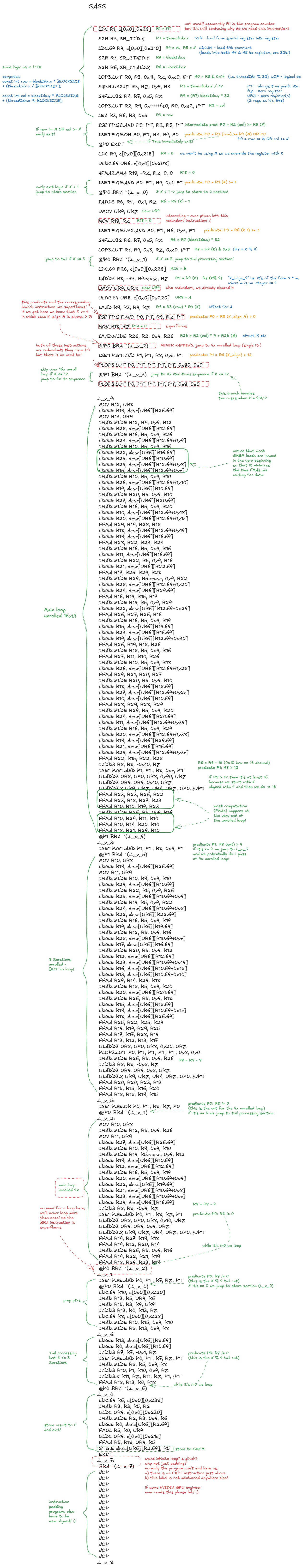
I'll just highlight the diffs compared to the PTX code:
- The loop is now unrolled ×16!
- LDG instructions are moved to the top of the loop, overlapping computation with data loading. FMAs are mostly clustered toward the end of each unrolled chunk.
- There are 2 tail loops: one unrolled 8x, one unrolled 4x, and the final loop covers the last 3 iterations.
I found interesting compiler quirks and inefficiencies in SASS as well:
- The program counter (
R1register) is loaded but never used. Unclear why? - Redundant initializations to zero still remain.
- One predicate is a noop: it's always true, so the jump to label
L_x_2(4× unrolled loop) is never taken. - The 4× unrolled loop contains a superfluous
BRAinstruction — it will never iterate more than once. - After the final
EXIT, the code falls into an infinite while-loop. Spurious implementation detail or a glitch? - Finally (not a glitch), the code is padded with
NOPsfor memory alignment.
Fun! We got a feeling for what compilers do behind the scenes.
Now, with all of this background, let's shift gears and dive into some SOTA kernels.
Designing near-SOTA synchronous matmul kernel
In this chapter, we'll break down an fp32 kernel that is close to SOTA under the following constraints:
- No TMA
- No asynchronous memory instructions
- No tensor cores
- fp32 only (no bf16)
In other words, this is SOTA under a pre-Volta GPU model (and near SOTA on Volta/Ampere):
- Volta introduced tensor cores
- Ampere introduced async memory instructions
- Hopper introduced TMA
The technique we'll study is called warp-tiling.
Before we dive into that, let's revisit our previous kernel with a tiny modification and see what happens. Specifically, we'll change how the row and col variables are computed.
Original version:
const int row = blockIdx.x * BLOCKSIZE + (threadIdx.x / BLOCKSIZE);
const int col = blockIdx.y * BLOCKSIZE + (threadIdx.x % BLOCKSIZE);
Modified version:
const int row = blockIdx.x * BLOCKSIZE + (threadIdx.x % BLOCKSIZE);
const int col = blockIdx.y * BLOCKSIZE + (threadIdx.x / BLOCKSIZE);
In other words, we just swap the % and /operators.
Swapping row2 and col2 is the only change in the logical structure compared to the previous example:
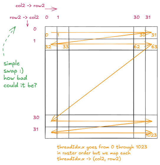
And here's what the modified kernel does now:
That seemingly harmless tweak makes our GMEM access non-coalesced.
On my H100 PCIe card, performance dropped from 3171 GFLOP/s to just 243 GFLOP/s — a 13× slowdown. Exactly the kind of penalty we saw earlier in the GMEM section (the Stephen Jones strided GMEM access experiment).
From the outside, it looks like just a trivial swap between two operators. But if you don't have a mental model of the hardware, you'd never expect such a dramatic effect.
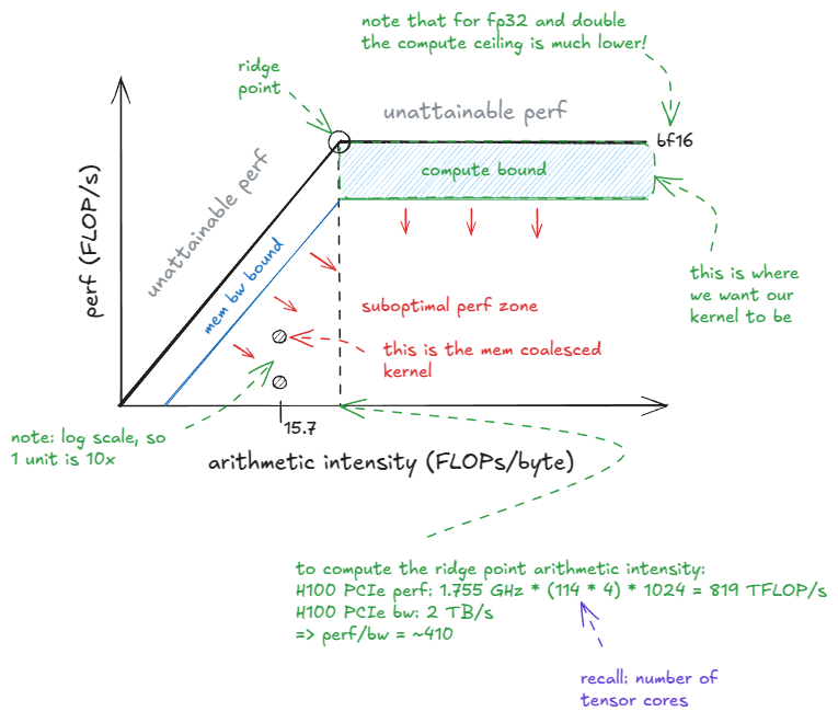
Looking at the roofline model, you can see that our kernel sits deep in the memory-bandwidth-bound region of the plot. We're paying NVIDIA big bucks for compute, so we might as well aim for the compute-bound zone.
The roofline model plots performance (FLOP/s) on the y-axis against arithmetic intensity (AI) on the x-axis.
Arithmetic intensity is defined as the number of FLOPs performed per byte loaded from device memory / GMEM (by default).
The “ridge point” occurs at: peak perf / GMEM bw. For my H100 PCIe, this works out to ~410. Only once AI exceeds this value can the kernel enter the compute-bound regime.
Let's revisit the sequential matmul code before proceeding. For reference:
for (int m = 0; m < M; m++) {
    for (int n = 0; n < N; n++) {
        float tmp = 0.0f;  // accumulator for dot product
        for (int k = 0; k < K; k++) {
            tmp += A[m][k] * B[k][n];
        }
        C[m][n] = tmp;
    }
}
The key point I want to make here is that the semantics are invariant to loop order. In other words, we can permute the three nested loops in any of the 3! = 6 ways, and the result will still be a correct matmul.
Out of these six permutations, the most interesting is the one with K as the outermost loop. (The relative ordering of m and n is less important, so let's assume the "canonical" m-n order):
for (int k = 0; k < K; k++) {
    for (int m = 0; m < M; m++) {
        float a = A[m][k];  // reuse this load across N (think GMEM access minimization)
        for (int n = 0; n < N; n++) {
            C[m][n] += a * B[k][n];
        }
    }
}
If these loads were coming from GMEM, we've just saved roughly 2× bandwidth by reducing the number of loads for A from N^3 down to N^2.
But the more important insight is algorithmic: this version computes matmul as a partial sum of outer products. That perspective is crucial for understanding the warp-tiling method, which we'll dive into next:
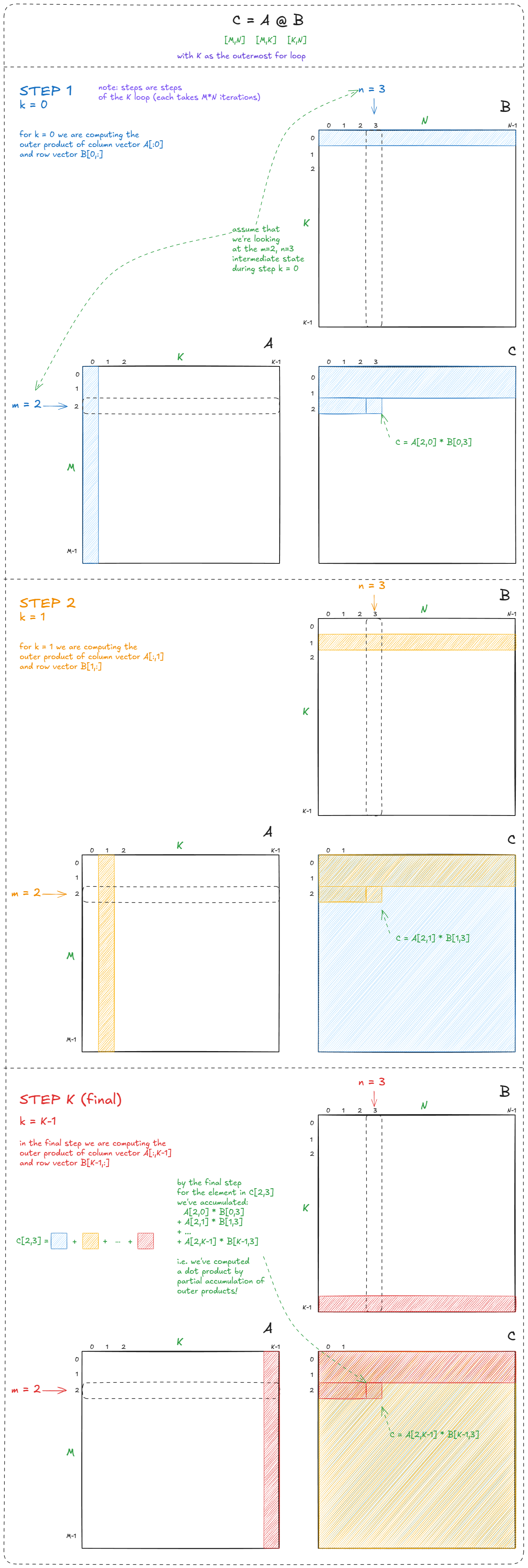
It may be obvious, but it's worth emphasizing: a dot product is equivalent to a sum of partial dot products:
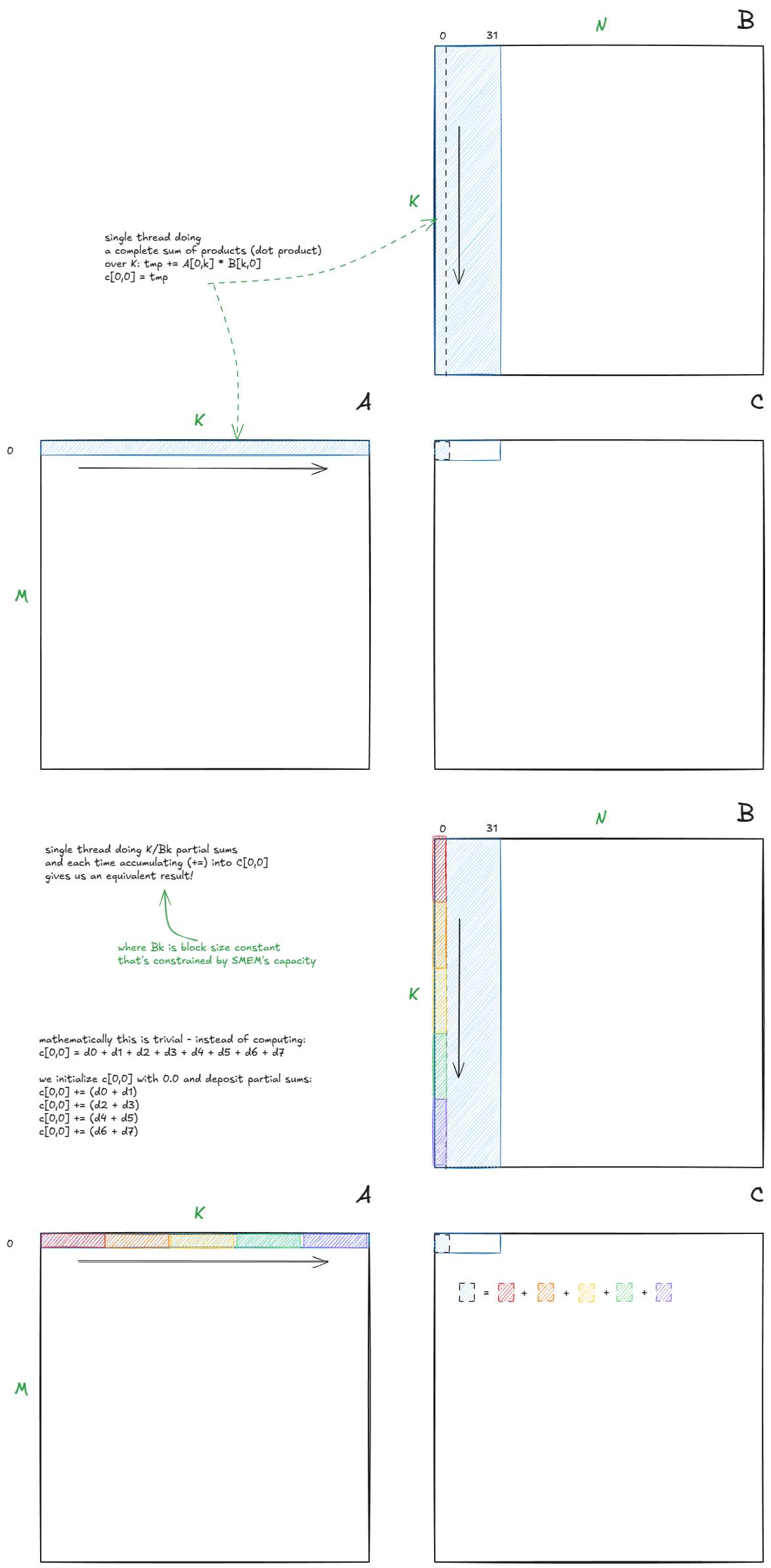
This matters because it lets us break the computation into a series of block matmuls (each producing partial dot products). By moving those blocks into SMEM before performing the computation, we can cut down on GMEM traffic and speed things up significantly.
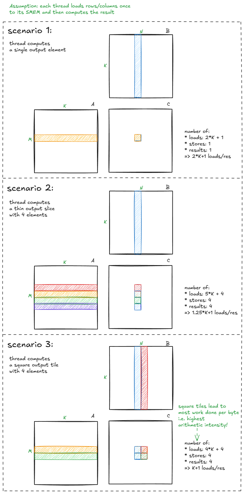
Recall also that our initial kernels had very low arithmetic intensity — they did little work per byte loaded. To improve it, we need to:
- Compute multiple output elements per thread.
- Make output tiles as square as possible.
Here's a visual intuition for why that matters:
At this point we've gathered most of the pieces needed to understand warp-tiling. Let's put them together.
We know two key things:
- Output tiles should be square (to maximize arithmetic intensity).
- The computation should be broken into substeps, so that intermediate chunks can fit into SMEM.
With that in mind, the high-level structure of the algorithm looks like this:
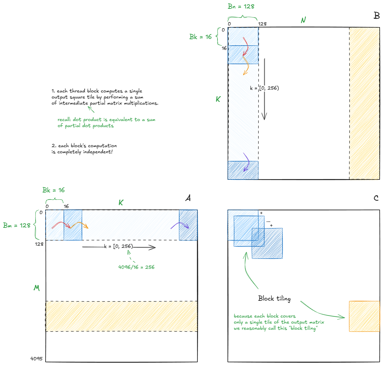
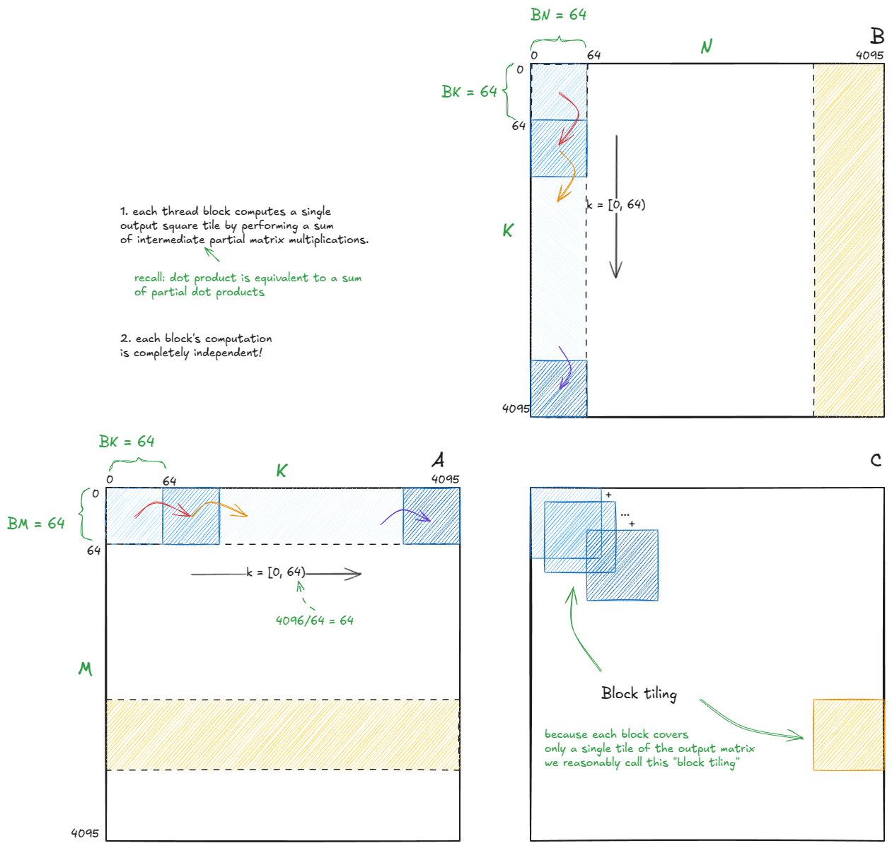
I'll use the same tile sizes as in Simon's blog post (not auto-tuned for my H100):
Bm = Bn = 128, Bk = 16
Since each block's computation is independent — and we've already convinced ourselves that partial dot products accumulate to the full dot product — we only need to focus on a single block's single step. The rest (the other 1023 blocks, 4096/128 * 4096/128 = 32 * 32 = 1024 total) will follow the same logic.
With that mindset, let's zoom into the first step (computation before the red arrow transition) of the blue block, which corresponds to output tile C[0,0] (notice - tile - not element).
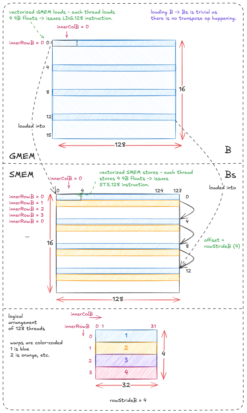
The chunk dimensions are Bm × Bk for matrix A and Bk × Bn for matrix B. These are loaded into SMEM buffers As and Bs.
Loading/storing B into Bs is straightforward because Bs is not transposed. Each of the 4 warps fetches a row of B from GMEM, with each thread issuing a vectorized load (LDG.128) followed by a vectorized store (STS.128). Each warp loops 4 times with a stride of 4 rows.
Corresponding code (I added comments and removed Simon's commented out code):
for (uint offset = 0; offset + rowStrideB <= BK; offset += rowStrideB) {
    // we need reinterpret_cast to force LDG.128 instructions (128b = 4 4B floats)
    reinterpret_cast<float4 *>(
        &Bs[(innerRowB + offset) * BN + innerColB * 4])[0] =
        reinterpret_cast<const float4 *>(
            &B[(innerRowB + offset) * N + innerColB * 4])[0];
  }
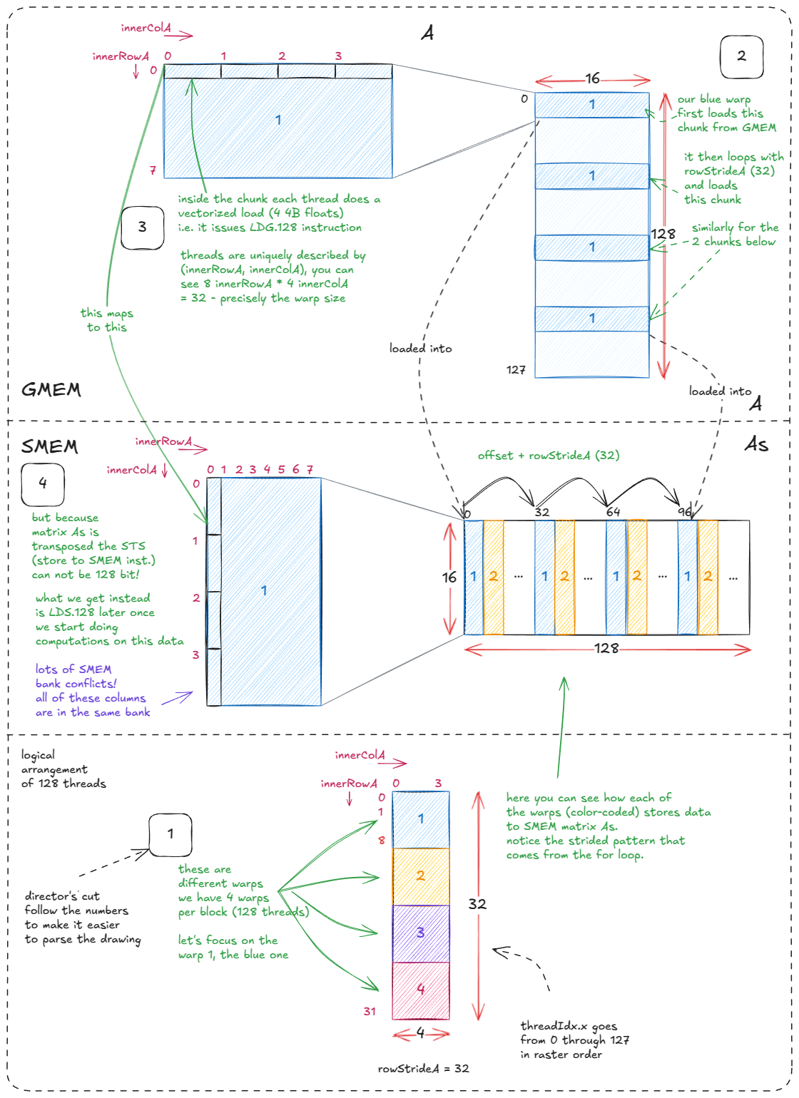
Loading A → As. This step is trickier because As is transposed. The reason for the transpose is that it enables vectorized loads (LDS.128) later during the compute phase.
The trade-off is that the stores cannot be vectorized: the 4 floats fetched from a row of A must now be scattered into a column of As, which maps into the same memory bank. That's acceptable because we prioritize fast loads — each element of As will be accessed multiple times during computation, while the stores happen only once.
The innerRowX and innerColX annotations in the diagram show exactly which work each thread is responsible for.
Corresponding code:
for (uint offset = 0; offset + rowStrideA <= BM; offset += rowStrideA) {
  // we need reinterpret_cast to force LDG.128 instructions
  const float4 tmp = reinterpret_cast<const float4 *>(
      &A[(innerRowA + offset) * K + innerColA * 4])[0];
  As[(innerColA * 4 + 0) * BM + innerRowA + offset] = tmp.x;
  As[(innerColA * 4 + 1) * BM + innerRowA + offset] = tmp.y;
  As[(innerColA * 4 + 2) * BM + innerRowA + offset] = tmp.z;
  As[(innerColA * 4 + 3) * BM + innerRowA + offset] = tmp.w;
}
After loading, we synchronize the thread block (__syncthreads()) to ensure that all data is available in As and Bs.
Now comes the computation phase.
Corresponding code (I suggest skimming it and checking out the drawing with few passes between the two :)):
for (uint dotIdx = 0; dotIdx < BK; ++dotIdx) {  // dotIdx is the outer most loop
  // WM = 64, that's why As is broken into 2x64 parts
  // TM = 8, that's why thread processes 8 rows from As
  // WMITER = 1, that's why only single slice in As (2 in the appendix of the drawing)
  for (uint wSubRowIdx = 0; wSubRowIdx < WMITER; ++wSubRowIdx) {
    // load from As into register regM
    for (uint i = 0; i < TM; ++i) {
      regM[wSubRowIdx * TM + i] =
          As[(dotIdx * BM) + warpRow * WM + wSubRowIdx * WSUBM +
              threadRowInWarp * TM + i];
    }
  }
  // WN = 64, that's why Bs is broken into 2x64 parts
  // TN = 4, that's why 4 columns per slice of Bs
  // WNITER = 4, that's why four slices in Bs
  // WSUBN = WN/WNITER = 16 (used to iterate over slices)
  for (uint wSubColIdx = 0; wSubColIdx < WNITER; ++wSubColIdx) {
    for (uint i = 0; i < TN; ++i) {
      // load from Bs into register regN
      regN[wSubColIdx * TN + i] =
          Bs[(dotIdx * BN) + warpCol * WN + wSubColIdx * WSUBN +
              threadColInWarp * TN + i];
    }
  }

  // execute warptile matmul via a sum of partial outer products
  for (uint wSubRowIdx = 0; wSubRowIdx < WMITER; ++wSubRowIdx) {
    for (uint wSubColIdx = 0; wSubColIdx < WNITER; ++wSubColIdx) {
      for (uint resIdxM = 0; resIdxM < TM; ++resIdxM) {
        for (uint resIdxN = 0; resIdxN < TN; ++resIdxN) {
          threadResults[(wSubRowIdx * TM + resIdxM) * (WNITER * TN) +
                        (wSubColIdx * TN) + resIdxN] +=
              regM[wSubRowIdx * TM + resIdxM] *
              regN[wSubColIdx * TN + resIdxN];
        }
      }
    }
  }
}
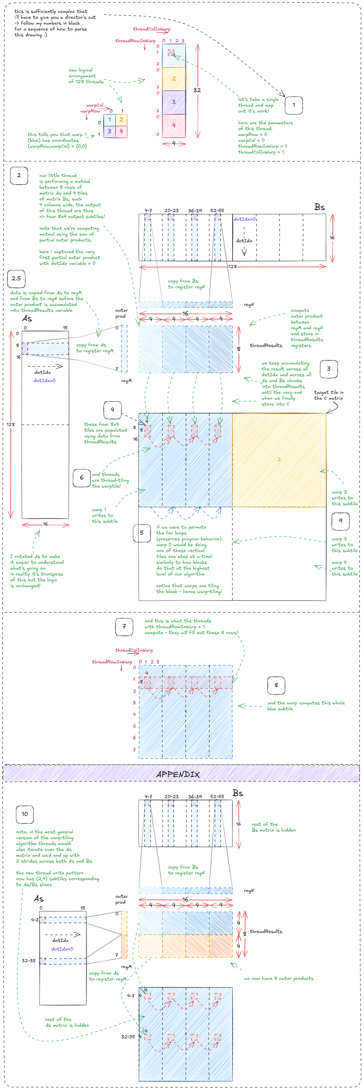
Once the chunk is processed, we synchronize again. This prevents race conditions — without it, some threads could start writing the next chunks into As and Bs while others are still working on the current ones.
After synchronization, we advance the pointers for A and B by Bk, and the algorithm repeats until all chunks are processed.
A += BK;     // move BK columns to right
B += BK * N; // move BK rows down
Finally, once the loop completes, the 128 threads flush their private threadResults registers into the corresponding output tile of matrix C (that by now contain the full dot product!).
In practice, you'd autotune the parameters of this algorithm for your specific GPU. But as noted earlier, this style of kernel is no longer the method of choice — modern GPUs have asynchronous memory mechanisms and tensor cores that push performance far beyond what warp-tiling alone can deliver.
With that, let's move on to true SOTA on Hopper.
I highly recommend Pranjal's excellent blog post [15], which reads more like a worklog. In this chapter, I'll be following kernels from his worklog. As with Simon's work, much of the code appears to be CUTLASS-inspired (see, for example, these posts: CUTLASS ping pong kernel [16] and efficient GEMM).
Notably, devil is in the details and Pranjal managed to outperform cuBLAS SOTA — hitting ~107% of cuBLAS performance on a few target matrix dimensions.
Designing SOTA asynchronous matmul kernels on Hopper
Now it's time to bring out all the hardware features and reach true SOTA on Hopper. We'll be using:
- TMA sync load/store operations
- Tensor Cores
- bf16 precision
These hardware features both significantly simplify the warp-tiling method and boost performance by nearly an order of magnitude — Pranjal reported a 10x increase from 32 TFLOP/s to 317 TFLOP/s.
The reason this simplification works is that TMA and Tensor Cores abstract away much of the manual complexity we wrestled with earlier.
As a first step toward Hopper SOTA, let's modify the warp-tiling baseline.
We keep the exact same program structure, except that:
- We now need only 128 threads (4 warps) per thread block.
- Tile sizes are set to
BM = BN = BK = 64.
Async load into SMEM via TMA
For the second stage — loading data into SMEM — TMA replaces the intricate warp-level loading pattern with something much simpler. All we need to do is:
- Construct tensor maps for
AandB. - Trigger TMA operations (done by a single thread in the block).
- Synchronize using shared-memory barriers.
TMA not only moves the data but also applies swizzling automatically, which resolves the bank conflicts we previously saw in warp-tiling. (I'll cover swizzling in detail in a dedicated section later.)
To form a tensor map, we use cuTensorMapEncodeTiled (see docs). This function encodes all the metadata needed to transfer chunks of A and B from GMEM into SMEM. We need one tensor map per A and B, but structurally they're the same. For A, we specify:
- Data type: bf16
- Rank: 2 (matrix)
- Pointer:
A - Shape:
(K,M)(fastest stride dimension first) - Row stride:
K * sizeof(bf16) sA's shape:(BK, BM)- Swizzle mode: use 128B pattern when loading into
sA
Next:
__shared__ barrier barA;  // SMEM barriers for A and B
__shared__ barrier barB;

if (threadIdx.x == 0) {
    // initialize with all 128 threads
    init(&barA, blockDim.x);
    init(&barB, blockDim.x);
    // make initialized barrier visible to async proxy
    cde::fence_proxy_async_shared_cta();
}
__syncthreads();  // ensure barriers are visible to all threads
Here we initialize SMEM barriers that will synchronize writes into sA and sB. The barriers are initialized with all 128 threads, since we expect every thread in the block to reach the barrier before it can flip to the “ready” state.
The call to cde::fence_proxy_async_shared_cta() is part of Hopper's proxy memory model. It orders visibility between the "async proxy" (TMA) and the "generic proxy" (normal thread ld/st) at CTA (block) scope. Here we issue it immediately after initialization so the async engine sees the barrier's initialized state. (Completion of async copies will be signaled by the mbarrier itself.)
In the outer K-loop:
for (int block_k_iter = 0; block_k_iter < num_blocks_k; ++block_k_iter) {
    if (threadIdx.x == 0) {  // only one thread launches TMA
        // Offsets into GMEM for this CTA's tile:
        //   A: (block_k_iter * BK, num_block_m * BM)
        cde::cp_async_bulk_tensor_2d_global_to_shared(
            &sA[0], tensorMapA, block_k_iter*BK, num_block_m*BM, barA);
        // update barrier with the number of bytes it has to wait before flipping:
        // sizeof(sA)
        tokenA = cuda::device::barrier_arrive_tx(barA, 1, sizeof(sA));
        //   B: (block_k_iter * BK, num_block_n * BN)
        cde::cp_async_bulk_tensor_2d_global_to_shared(
            &sB[0], tensorMapB, block_k_iter*BK, num_block_n*BN, barB);
        tokenB = cuda::device::barrier_arrive_tx(barB, 1, sizeof(sB));
    } else {
        tokenA = barA.arrive();  // threads-only arrival (no byte tracking)
        tokenB = barB.arrive();
    }
    barA.wait(std::move(tokenA));  // blocks until: all threads arrived AND TMA finished
    barB.wait(std::move(tokenB));
What's happening, step by step (for both A and B):
- Thread 0 launches TMA with
cp_async_bulk_tensor_2d_global_to_shared(...), specifying the SMEM destination (sA/sB), the tensor map, and the GMEM offsets specify the source GMEM chunk. - It immediately calls
barrier_arrive_tx(bar, 1, sizeof(sX)), which: - counts thread arrivals (1 here, from thread 0), and
- arms the barrier with the expected byte count so it knows when the async copy is complete.
- All other threads call
bar.arrive(), contributing their arrivals (no bytes). - Every thread then calls
bar.wait(token). This wait completes only when both conditions are true: - all 128 threads have arrived, and
- the async engine has written all
sizeof(sX)bytes into shared memory.
This load pattern is the standard Hopper idiom — you'll see it all over modern kernels.
During the async copy, TMA also swizzled the data using the 128B swizzle format.
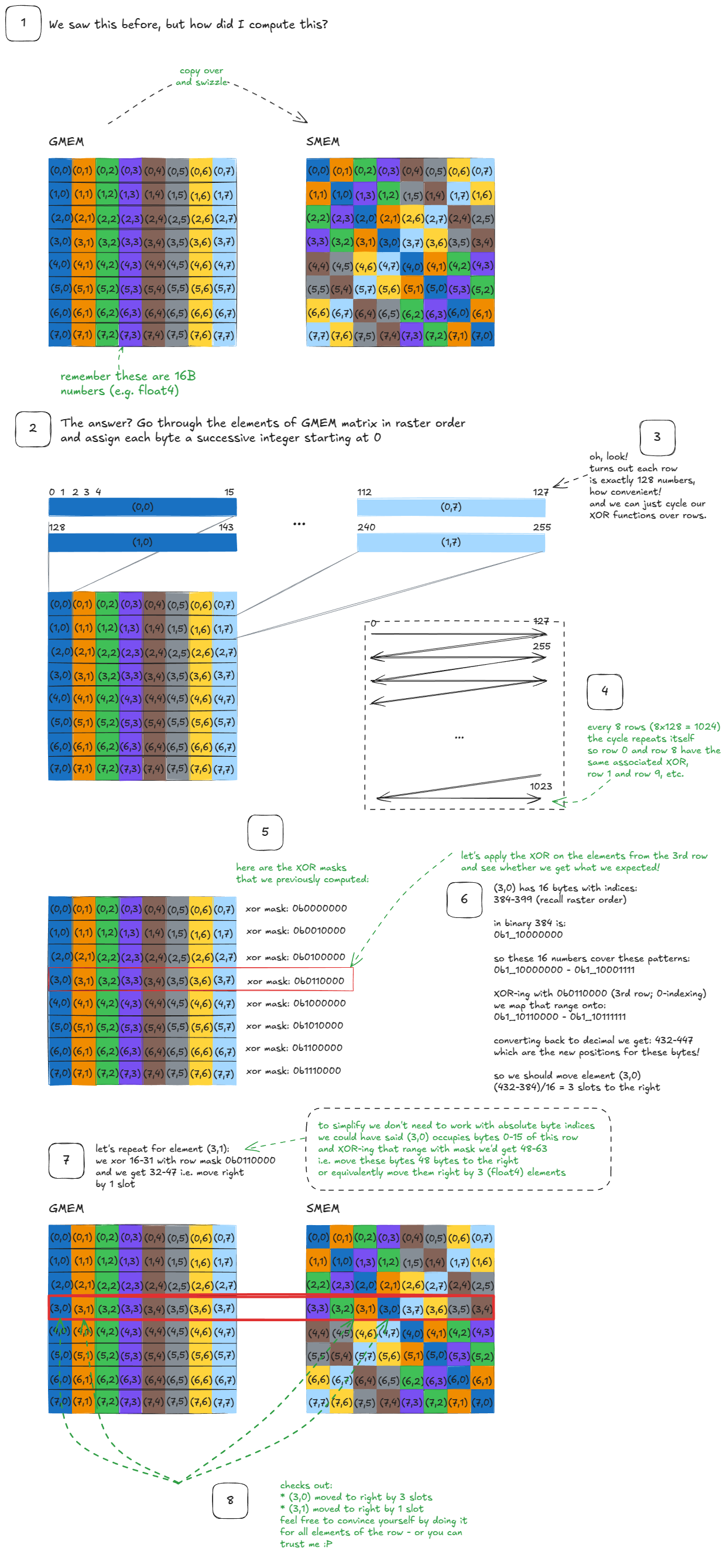
Let's take a moment to unpack what swizzling actually means. I couldn't find a clear explanation online, so here's my attempt — partly for you, partly for my future self. :)
Swizzling
Let's start with a motivating example:
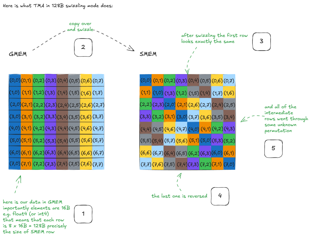
What's happening here?
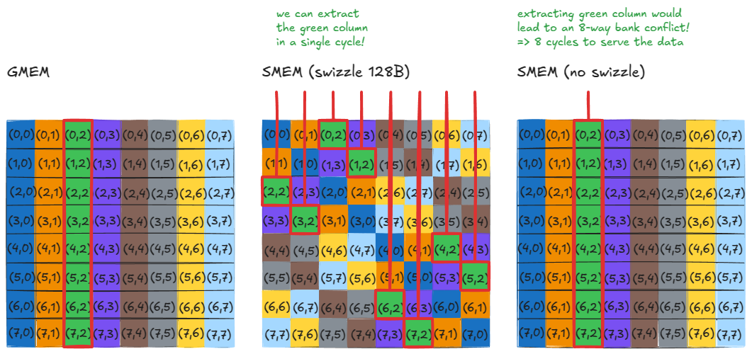
Suppose we want to load all elements from the first row of the original GMEM matrix. After swizzling, that's still trivial: just read the first row from the SMEM matrix. Nothing special there.
Now, suppose we want the first column of the original GMEM matrix. Notice that these elements now lie along the diagonal in SMEM. That means we can load them in a single cycle, since no two threads hit the same bank — zero bank conflicts.
Without swizzling, this access would map all those column elements into the same bank but different addresses, producing an 8-way bank conflict and slashing throughput by 8x.
The same property holds for any row or column: after swizzling, they can all be served in a single cycle!
The same property holds for stores. For example, if you wanted to transpose a matrix in SMEM, the naïve way would be: load a row and then write it back as a column. Without swizzling, that would cause an 8-way bank conflict.
With swizzling enabled, we escape this problem, but you do have to be careful with indexing.
So now that the motivation is clear, let's ask the following question: how does TMA actually generate the swizzle pattern?
It turns out the answer is simple: XOR with a specific mask pattern.
Quick reminder on XOR, here is the truth table:
- 0, 0 maps to 0
- 0, 1 maps to 1
- 1, 0 maps to 1
- 1, 1 maps to 0
Notably: when one of the bits is 1, XOR flips the other bit.
As usual, we can find the answer in CUTLASS. Another Simon (not the one from earlier) also gave a nice explanation of how the mask pattern is generated [18] — though not exactly how that pattern leads to the specific swizzle layouts we just saw.
So two big questions remain:
- How is the XOR mask generated?
- How is the mask actually applied to produce the swizzle pattern?
Generating the XOR mask
NVIDIA associates each swizzle mode with a particular “swizzle function”:
- 128B swizzle mode is associated with
Swizzle<3,4,3> - 64B swizzle mode is associated with
Swizzle<2,4,3> - 32B swizzle mode is associated with
Swizzle<1,4,3>
Let's unpack Swizzle<3,4,3>. I'll then share the XOR masks for the others.
// To improve readability, I'll group bits in 8s with underscores.

// Swizzle<3, 4, 3>
// -> BBits = 3
// -> MBase = 4
// -> SShift = 3

// Given the decoded arguments from above here are the steps that the swizzling function does:

// Step 1. Compute bit_msk = (1 << BBits) - 1
bit_msk = (0b00000000_00000001 << 3) - 1 = 0b00000000_00000111  // keep 16 bit resolution

// Step 2. Compute yyy_msk = bit_msk << (MBase + max(0, SShift))
yyy_msk = 0b00000000_00000111 << 7 = 0b00000011_10000000

// Step 3. Mask the input number (annotated bits A-P for clarity)
input_number = 0bABCDEFGH_IJKLMNOP

masked = input_number & yyy_mask
  = 0bABCDEFGH_IJKLMNOP & 0b00000011_10000000 = 0b000000GH_I0000000

// Step 4. Shift right by SShift (masked >> SShift)
shifted = masked >> 3
  = 0b000000GH_I0000000 >> 3 = 0b00000000_0GHI0000

// Step 5. XOR with the original input
output = input_number ^ shifted
  = 0bABCDEFGH_IJKLMNOP ^ 0b00000000_0GHI0000 = 0bABCDEFGH_IwyzMNOP

// Replace unchanged bits with x for legibility.
// I'll also uppercase "wyz" to make it stand out and keep GHI around as they have an impact on wyz:
output = 0bxxxxxxGH_IWYZxxxx

// where WYZ = GHI ^ JKL (XOR)
In plain language: The swizzle function looks at bits GHI (positions 9, 8, 7, zero-indexed). If any of these are 1, it flips the corresponding bits JKL (positions 6, 5, 4) to get WYZ. All other bits are untouched.
Let's build some intuition for how the swizzling function behaves:
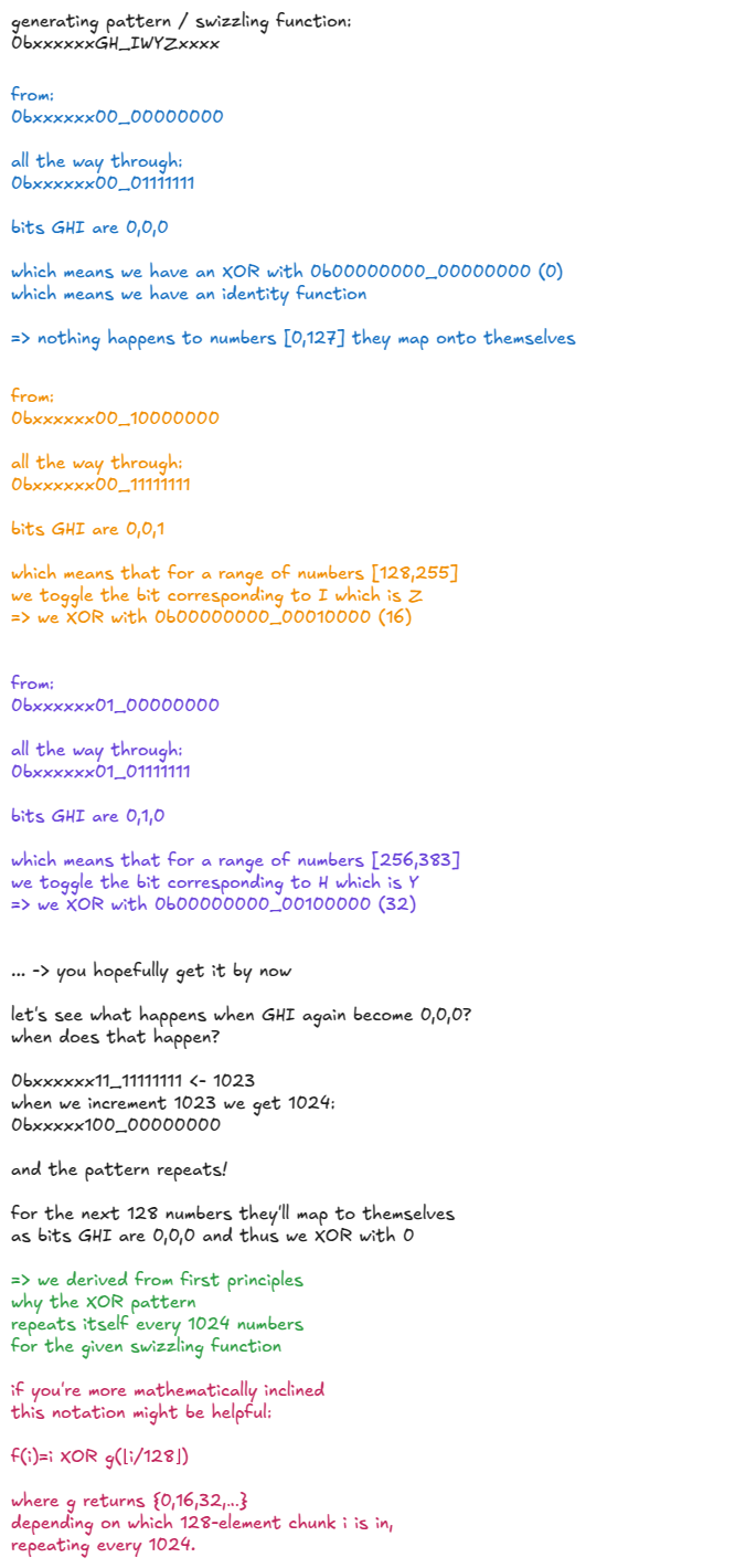
For 32B and 64B swizzling modes the swizzling functions are 0bxxxxxxxx_IxxZxxxx and 0bxxxxxxxH_IxYZxxxx.
These follow the same XOR-with-mask idea, just with different control bits driving which lower bits get flipped.
How does all this connect back to the motivating example we started with?
Here's the link:
And that's both the WHY and the HOW of swizzling. :)
Tensor Cores
Back to tensor cores. At this point, we've got chunks of A and B pulled from GMEM into sA and sB in SMEM. They're swizzled, and ready for tensor core consumption.
NVIDIA exposes several matrix-multiply-accumulate (MMA) instructions:
wmma— warp-cooperative, synchronous (older generations).mma.sync— warp-cooperative, synchronous (Ampere).wgmma.mma_async— warp-group cooperative, asynchronous (Hopper).
We'll focus on wgmma.mma_async (docs [19]), since it was introduced with Hopper and is by far the most powerful. It's asynchronous and leverages 4 collaborating warps to compute the matmul together; precisely the reason why we chose our block size = 128.
For bf16 operands, wgmma supports shapes of the form m64nNk16, where N ∈ {8, 16, 24, …, 256}. In our current example we'll use m64n64k16, but in general, larger N values are more performant (as long as you have enough registers and SMEM to back them).
m64n64k16 means the tensor core computes a 64×16 × 16×64 matmul in one go.The following are the operand placement rules: sA can reside in registers or in SMEM, sB must reside in SMEM, and the accumulator (BM x BN) always in registers.
Since that's far too many registers for a single thread, the accumulator is partitioned across threads in the warp group.
In our reference kernel you'll see it initialized like this:
float d[WGMMA_N/16][8];  // d is the accumulator; GEMM: D = A @ B + D
memset(d, 0, sizeof(d));  // init to all 0s
We set WGMMA_M = WGMMA_N = BM = BN = 64. That gives:
- 128 threads in the warp group
- Each thread holds
WGMMA_N/16 × 8registers - In total: 128 × (64/16) × 8 = 64 × 64 registers
...which matches exactly the accumulator size (BM × BN = 64 × 64), just distributed across the group.
Here's the corresponding tensor core snippet we'll break down:
asm volatile("wgmma.fence.sync.aligned;" ::: "memory");
wgmma64<1, 1, 1, 0, 0>(d, &sA[0], &sB[0]);
wgmma64<1, 1, 1, 0, 0>(d, &sA[WGMMA_K], &sB[WGMMA_K]);
wgmma64<1, 1, 1, 0, 0>(d, &sA[2*WGMMA_K], &sB[2*WGMMA_K]);
wgmma64<1, 1, 1, 0, 0>(d, &sA[3*WGMMA_K], &sB[3*WGMMA_K]);
asm volatile("wgmma.commit_group.sync.aligned;" ::: "memory");
asm volatile("wgmma.wait_group.sync.aligned %0;" ::"n"(0) : "memory");
- Some Hopper instructions aren't exposed in CUDA C++, so we drop into inline PTX with
asm(...);. ::: "memory"is a memory clobber, it prevents any memory optimizations around the asm statement, it's a "don't move surrounding memory accesses past this point" hint to the compiler; disallowing the compiler to shuffle memory ops around this statement.volatiletells the compiler the asm block *must not* be deleted or hoisted, even if it looks redundant (see docs) [20].
Let's first unpack the bookend instructions (wgmma.fence, commit_group, wait_group) that surround the actual matmul calls.
wgmma.fence.sync.aligned; - The docs explain it pretty well: "wgmma.fence establishes an ordering between prior accesses to any warpgroup registers and subsequent accesses to the same registers by a wgmma.mma_async instruction."
In practice, all four warps of the warp-group have to execute this fence before the very first wgmma.mma_async.
After that, we're good to go. Even though the accumulator registers are being updated across those four wgmma calls, we don't need more fences in between — there's a special exception for back-to-back MMAs of the same shape accumulating into the same registers. That's exactly our situation here.
It's really just boilerplate. In fact, if you comment it out, the compiler will quietly slip it back in for you.
wgmma.commit_group - another boilerplate operation: from the docs "Commits all prior uncommitted wgmma.mma_async operations into a wgmma-group". It closes off all the wgmma.mma_async we just launched (four calls above) into a single "group".
wgmma.wait_group 0 - means: don't go any further until every group prior to this point has finished. Since we only launched one group here, it's just saying "hold on until those four MMAs are done and the results are actually sitting in the accumulator registers".
So the standard rhythm is: fence → fire off a batch of async MMAs → commit them → wait for them to finish.
Now onto the wgmma itself. wgmma64 function is a wrapper around inline PTX call:
wgmma.mma_async.sync.aligned.m64n64k16.f32.bf16.bf16The structure of the opcode makes its meaning fairly transparent: f32 is the accumulator datatype, and bf16 are the datatypes of the input sA and sB matrices.
The semantics are the usual fused multiply-accumulate: D = A @ B+D that is, GEMM accumulation into the existing fp32 tile. (There is a flag that can turn it into D=A @ B, we'll use it later.)
sA and sB are formed and passed into the instruction. These descriptors encode the SMEM base address, the swizzle mode (128B in our case), and LBO/SBO (leading/stride dim byte offset) values so the tensor core can navigate the layout correctly. Covering descriptor construction here would be a detour in an already lengthy post; it may deserve a focused write-up of its own. Just be aware that there are this additional metadata layer whose explanation I've omitted (for now).Here is an explanation of why we need 4 wgmma calls:
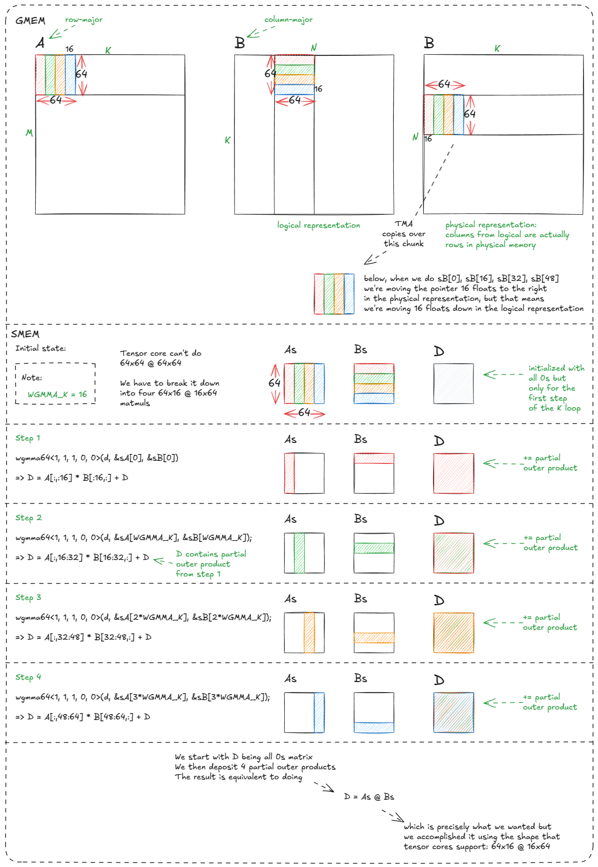
The slightly mind-bending part here is the column-major representation: how sB[0] … sB[48] ends up mapping to the correct logical positions/slices.
But the key takeaway is that much of the warp-tiling and thread-tiling complexity we wrestled with earlier is now abstracted away in hardware. What used to require careful orchestration across warps has collapsed into a handful of boilerplate instructions and a few declarative wgmma calls.
That said, this is only the starting point. We are still wasting both TMA and tensor core cycles:
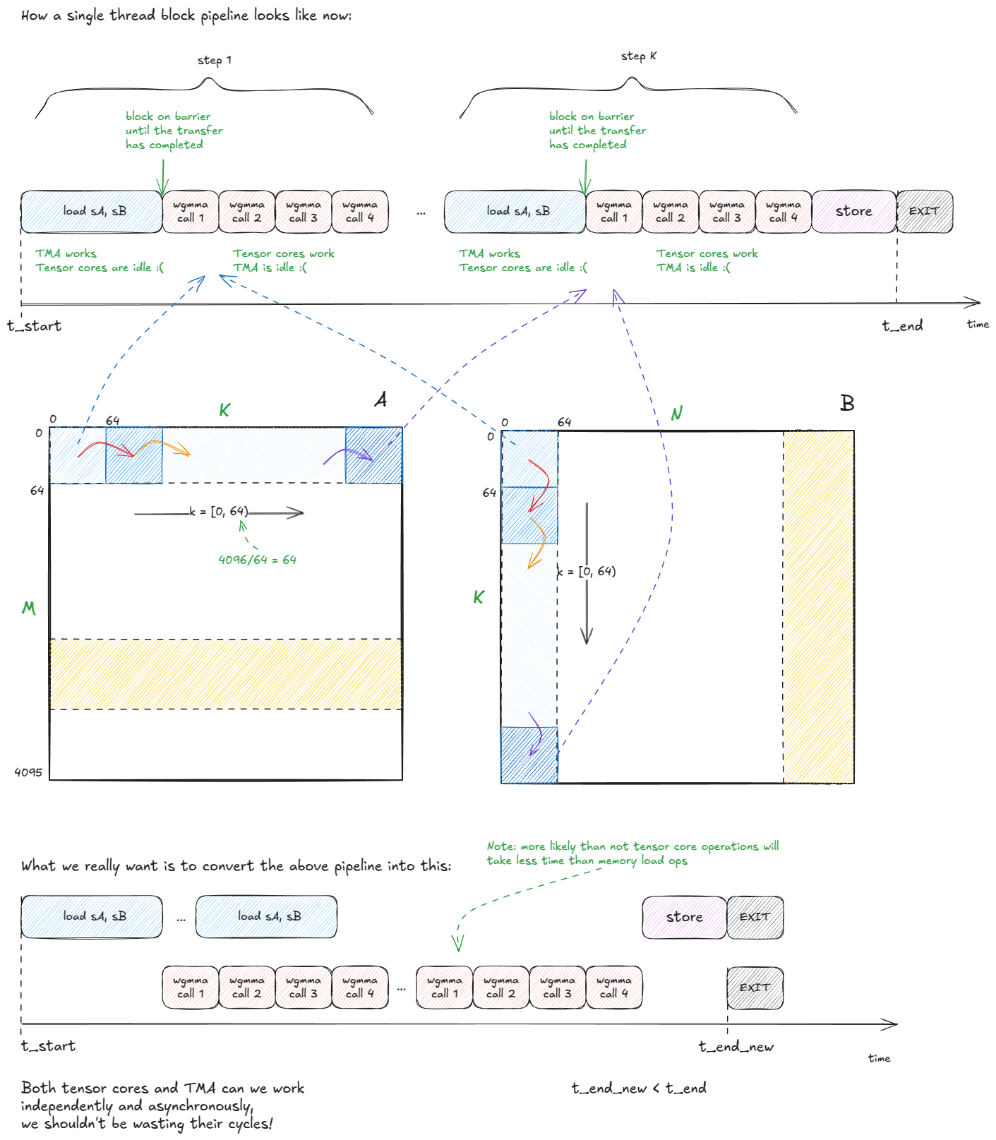
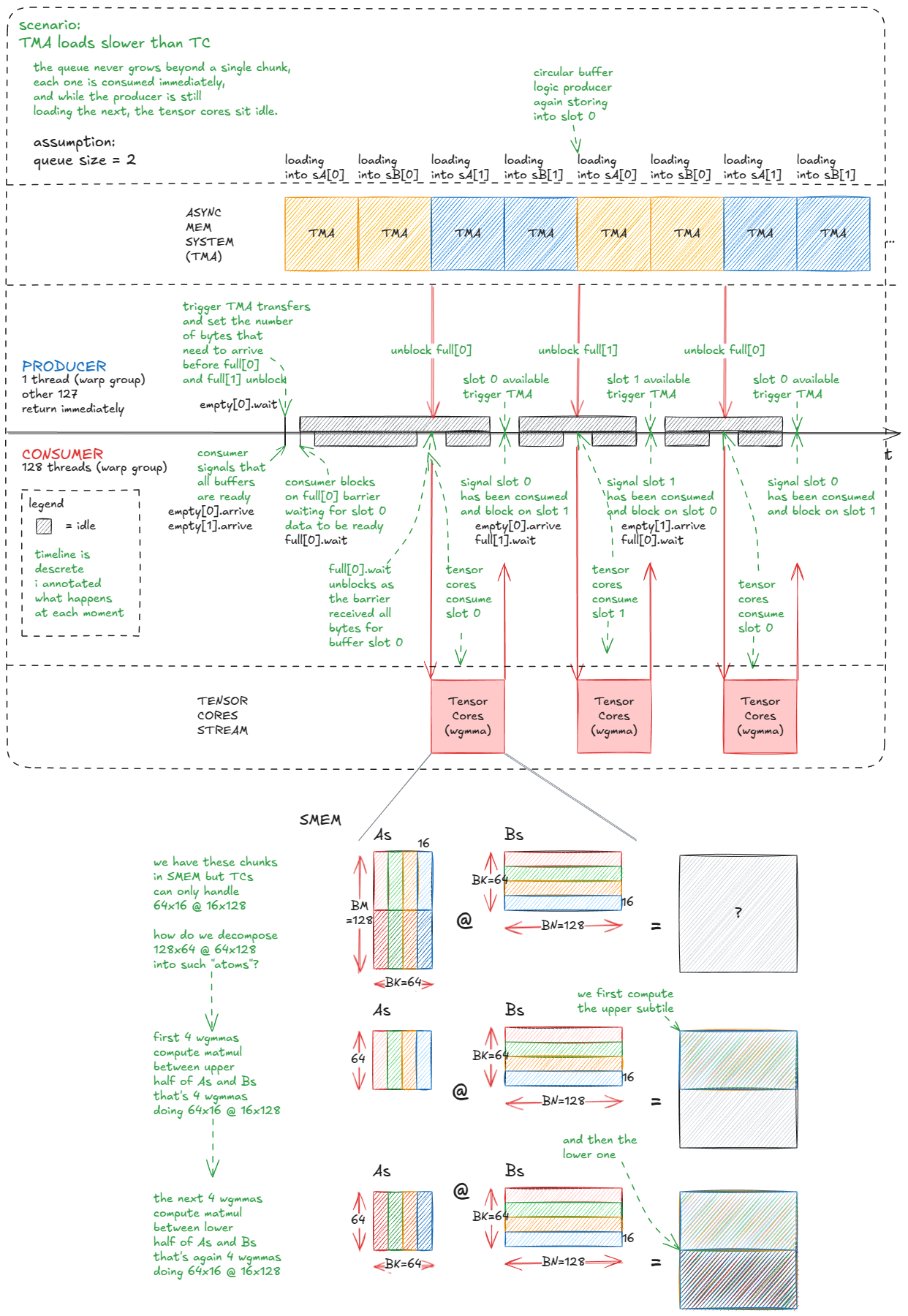
The way we address the wasted cycles is by pipelining compute and data movement. Concretely, we turn sA and sB (the SMEM-resident tiles) into a queue of chunks — say of length 5.
We then split the work across two warp-groups:
- One warp-group acts as the
producer, responsible for keeping TMA busy by streaming new chunks ofAandBinto the queue. - The other warp-group acts as the
consumer, drawing from the queue to keep the tensor cores saturated.
Naturally, this requires coordination. The mechanism we use is a queue of SMEM barriers, with one full[i]/empty[i] pair per slot in the queue to synchronize producer and consumer.
Here's the setup:
// queue of barriers
__shared__ barrier full[QSIZE], empty[QSIZE];
// use the largest MMA shape available
constexpr int WGMMA_M = 64, WGMMA_K = 16, WGMMA_N=BN;
Initialization is similar to before:
if (threadIdx.x == 0) {
  for (int i = 0; i < QSIZE; ++i) {
      // num_consumers == 1 in this example;
      // 128 threads from consumer wg + 1 producer thread
      init(&full[i], num_consumers * 128 + 1);
      init(&empty[i], num_consumers * 128 + 1);
  }
  cde::fence_proxy_async_shared_cta();  // same as before
}
__syncthreads();  // same as before
Two things to note:
- We've upgraded to a larger tensor core MMA (from
m64n64k16tom64nBNk16) as emprically it helps maximize the compute throughput. - Because the queue is multi-slot, the barrier initialization has to loop over all entries.
Here is the main logic:
- In the producer (
wg_idx = 0) one thread orchestrates TMA copies into the queue. It usesempty[qidx].wait()to block until a buffer slot is free, then issuescp_async_bulk_tensor_2d_global_to_sharedfor bothsAandsB. Finally, it signals completion withbarrier_arrive_tx, which ties the barrier to the byte count of the copy. - In the consumer (
wg_idx > 0) all threads first mark every queue slot as "empty" (ready to be filled). Then, for eachK-step, they wait onfull[qidx], run the tensor core MMAs over that buffer, and once done, mark the slot as empty again.
// Producer
if (wg_idx == 0) {  // wg_idx = threadIdx.x / 128
    if (tid == 0) {  // only thread 0 issues TMA calls
        int qidx = 0;  // index into the circular buffer
        for (int block_k_iter = 0; block_k_iter < num_blocks_k; ++block_k_iter, ++qidx) {
            if (qidx == QSIZE) qidx = 0;  // wrap around
            // wait until this buffer is marked empty (ready to be written into)
            empty[qidx].wait(empty[qidx].arrive());
            // copy over chunks from A and B
            cde::cp_async_bulk_tensor_2d_global_to_shared(
                &sA[qidx*BK*BM], tensorMapA, block_k_iter*BK, num_block_m*BM, full[qidx]);
            cde::cp_async_bulk_tensor_2d_global_to_shared(
                &sB[qidx*BK*BN], tensorMapB, block_k_iter*BK, num_block_n*BN, full[qidx]);
            // mark barrier with the expected byte count (non-blocking)
            barrier::arrival_token _ = cuda::device::barrier_arrive_tx(
              full[qidx], 1, (BK*BN+BK*BM)*sizeof(bf16));
        }
    }
} else {
    // Consumer warp-group
    for (int i = 0; i < QSIZE; ++i) {
        // i initially, all buffers are considered empty; ready for write
        // all 128 consumer threads arrive on each barrier
        barrier::arrival_token _ = empty[i].arrive();
    }
    // distributed accumulator registers, zero-initialized
    float d[BM/WGMMA_M][WGMMA_N/16][8];
    memset(d, 0, sizeof(d));

    int qidx = 0;
    for (int block_k_iter = 0; block_k_iter < num_blocks_k; ++block_k_iter, ++qidx) {
        if (qidx == QSIZE) qidx = 0;  // wrap around
        // wait until TMA has finished filling this buffer
        full[qidx].wait(full[qidx].arrive());

        // core tensor core loop
        warpgroup_arrive();  // convenience wrapper around the PTX boilerplate
        #pragma unroll  // compiler hint (we saw this in PTX/SASS section)
        // submit as many tensor core ops as needed to compute sA @ sB (see drawing)
        for (int m_it = 0; m_it < BM/WGMMA_M; ++m_it) {
            bf16 *wgmma_sA = sA + qidx*BK*BM + BK*m_it*WGMMA_M;
            #pragma unroll
            for (int k_it = 0; k_it < BK/WGMMA_K; ++k_it) {
                wgmma<WGMMA_N, 1, 1, 1, 0, 0>(
                  d[m_it], &wgmma_sA[k_it*WGMMA_K], &sB[qidx*BK*BN + k_it*WGMMA_K]);
            }
        }
        warpgroup_commit_batch();
        warpgroup_wait<0>();

        // all 128 consumer threads mark buffer as consumed so producer can reuse it
        barrier::arrival_token _ = empty[qidx].arrive();
    }

    // finally: write accumulator d back to output matrix C

}
The visualization should make it much clearer:
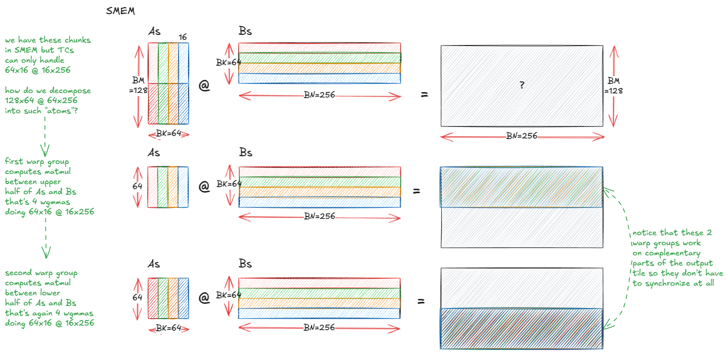
One natural tweak is to grow the output tile from 128×128 to 128×256. The catch is that at that size the per-thread accumulator shard in a single consumer warp-group becomes too large—each thread would need 256 fp32 registers just for the accumulator, which blows past the per-thread register budget (and triggers register spilling to device memory—which is very bad for performance).
The fix is to add another consumer warp-group so the accumulator is sharded across two groups instead of one. We keep a single producer (to drive TMA) and launch the block/CTA with 3×128 = 384 threads:
- WG0: producer (TMA)
- WG1: consumer A (computes the upper half of the 128×256 tile)
- WG2: consumer B (computes the lower half)
Each consumer owns a 64×256 half-tile of the output, so the per-thread accumulator footprint halves, avoiding spills.
Here is how the matmul is executed now:
The next big idea is that we can hide the latency of writing the output tile as well:
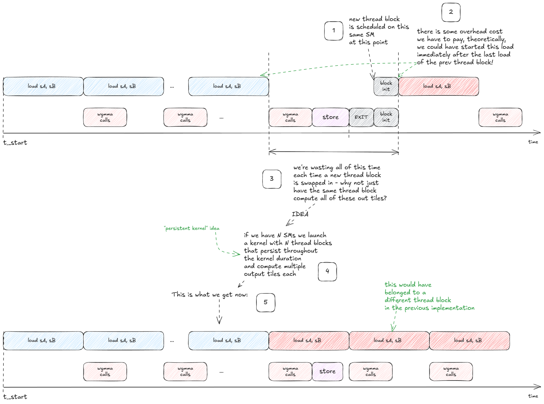
A persistent kernel launches a small, fixed number of thread blocks (often one per SM) and keeps them alive for the entire workload. Instead of launching a block per tile, each block runs an internal loop, pulling new tiles from a queue until the work is done.
That raises the natural question: which subset of output tiles should each SM process, and in what order?
How does this scheduling policy look like?
Let's start with a toy setup to reason about options:
- Total number of output tiles: 64.
- Number of SMs: 10.
- So each SM has to process ~6.4 blocks on average.
A first attempt might look like this:
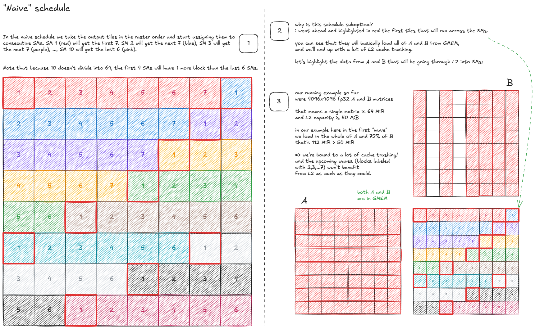
Can we do better? Yes—by making the schedule cache-aware:
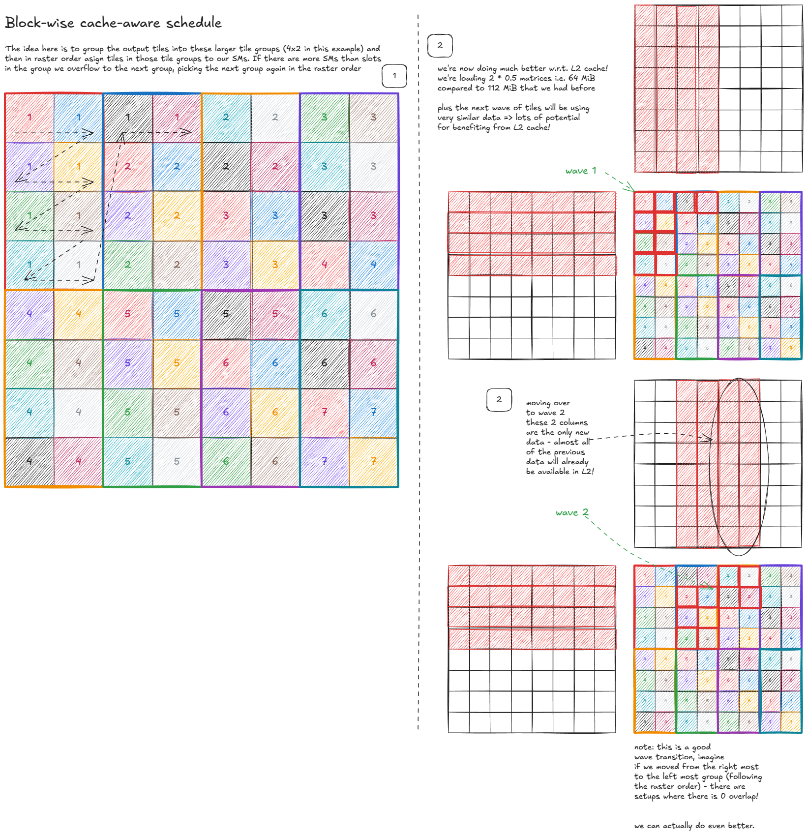
But can we do even better? Surprisingly, yes—by using a space-filling curve:
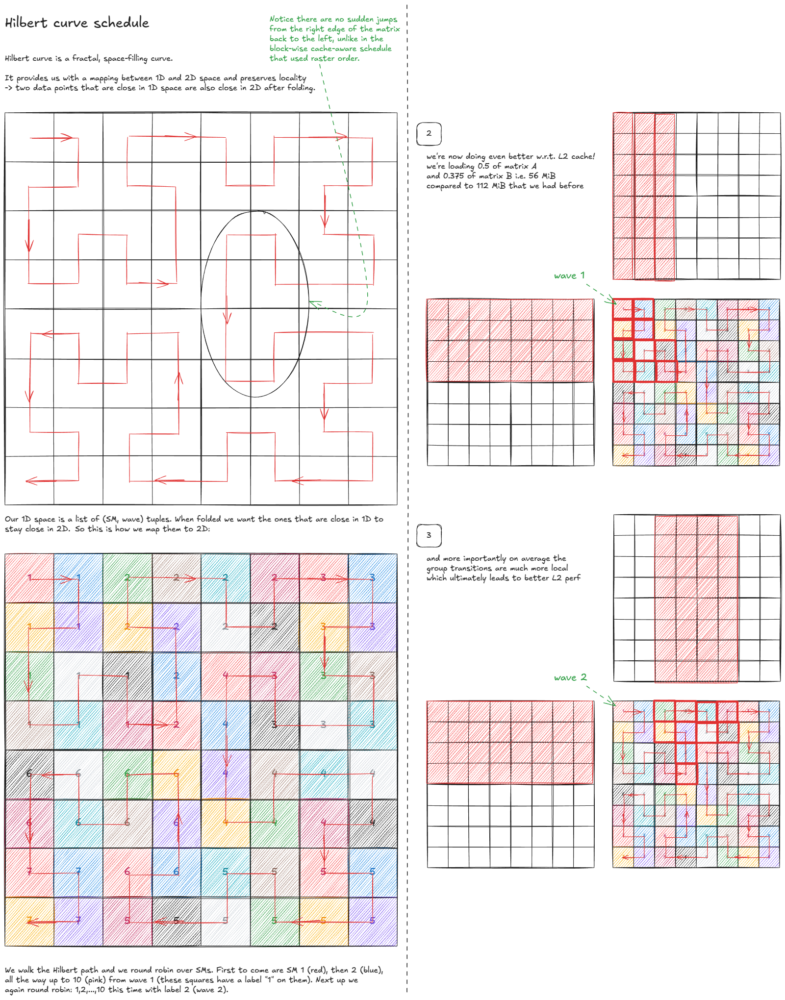
The final idea I'll cover in depth is to exploit Hopper's new cluster-level CUDA execution model to cut down on L2/GMEM traffic:
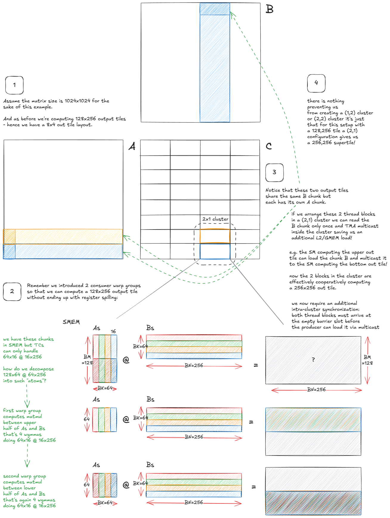
The key observation is that multiple SMs within a cluster can directly share their SMEM (via DSMEM), which lets us treat the cluster as a kind of "super-SM".
From the scheduling perspective, nothing radical changes: instead of each SM working on its own independent output tile, the entire cluster collaborates on a larger "super-tile". The mechanics of the algorithm remain the same, but now those SMs coordinate loads and reuse each other’s data.
And since the Hilbert-curve traversal was already designed to maximize locality, the super-SMs can follow the same traversal pattern — just at a coarser granularity.
Finally, to get past cuBLAS, we have to tighten up the synchronization itself. Up to this point we've been wasteful with arrive/wait calls on the barriers.
For example, consumer threads don't actually need to signal arrival on full[qidx]. The only condition that matters is "all bytes have arrived". Dropping those redundant arrivals saves 256 tokens per iteration. Similarly for empty[qidx]: once the consumers with tid==0 have arrived, the producer can safely start filling, since the consumer side (wgmma) executes in lock-step across all threads.
Few additional, lower-level tricks that add up in practice (in the spirit of O(NR)):
- Rebalance registers: use
asm volatile("setmaxnreg.{inc,dec}.sync.aligned.u32 %0;\n" : : "n"(RegCount));to shift register budget from the producer warp-group (lightweight) to the consumer warp-groups (heavy users during wgmma). - Avoid polluting caches on the way out. Either use
__stwtto bypass L1/L2, or better, do an async store: spill into SMEM first, then let TMA copy to GMEM asynchronously. This overlaps the write-back with compute, just like we did on the input side. - Skip redundant initialization: instead of zeroing the accumulator registers, adjust the tensor core sequence so that the first MMA does
C = A @ Band subsequent MMAs doC = A @ B + C.
For reference, here are the performance numbers (from Pranjal's blog) showing how each idea stacks on top of the previous ones:
| Optimization | Perf Before (TFLOP/s) | Perf After (TFLOP/s) |
|---|---|---|
| Baseline (warp-tiling) → Tensor Cores + TMA | 32 | 317 |
| Increase output tile size | 317 | 423 |
| Pipeline: overlap TMA loads with TC compute | 423 | 498 |
| Tile growth: 128×128 → 128×256 (2 consumer warp-groups) | 498 | 610 |
| Persistent kernels (hide store latency) | 610 | 660 |
| Faster PTX barriers | 660 | 704 |
| Clusters; TMA multicast | 704 | 734 |
| Micro-optimizations | 734 | 747 |
| TMA async stores (regs → SMEM → GMEM) | 747 | 758 |
| Hilbert-curve scheduling | 758 | 764 |
Additionally, Aroun submitted a PR that optimized the async store using the stmatrix method, yielding another +1%. A few nuclear reactors have been spared.
Epilogue
We began by dissecting the GPU itself, with an emphasis on the memory hierarchy — building mental models for GMEM, SMEM, and L1, and then connecting them to the CUDA programming model. Along the way we also looked at the "speed of light," how it's bounded by power — with hardware reality leaking into our model.
From there, we moved up the stack: learning how to talk to the hardware through PTX/SASS, and how to steer the compiler into generating what we actually want.
We picked up key concepts along the way — tile and wave quantization, occupancy, ILP, the roofline model — and built intuition around fundamental equivalences: a dot product as a sum of partial outer products, or as partial sums of dot products, and why square tiles yield higher arithmetic intensity.
With that foundation, we built a near-SOTA kernel (warp tiling) squeezing performance out of nothing but CUDA cores, registers, and shared memory.
Finally, we stepped into Hopper's world: TMA, swizzling, tensor cores and the wgmma instruction, async load/store pipelines, scheduling policies like Hilbert curves, clusters with TMA multicast, faster PTX barriers, and more.
I'll close on the belief that's carried me through this entire series: computers can be understood.
Acknowledgements
A huge thank you to Hyperstack for providing me with H100s for my experiments over the past year!
Thanks to my friends Aroun Demeure (GPU & AI at Magic, and ex-GPU architect at Apple and Imagination), and Mark Saroufim (PyTorch) for reading pre-release version of this blog post and providing feedback!
Get notified when I publish a new post.
References
- NVIDIA Hopper Architecture In-Depth https://developer.nvidia.com/blog/nvidia-hopper-architecture-in-depth/
- NVIDIA Ampere Architecture In-Depth https://developer.nvidia.com/blog/nvidia-ampere-architecture-in-depth/
- Strangely, Matrix Multiplications on GPUs Run Faster When Given "Predictable" Data! [short] https://www.thonking.ai/p/strangely-matrix-multiplications
- How CUDA Programming Works https://www.nvidia.com/en-us/on-demand/session/gtcfall22-a41101/
- Notes About Nvidia GPU Shared Memory Banks https://feldmann.nyc/blog/smem-microbenchmarks
- CUDA Binary Utilities https://docs.nvidia.com/cuda/cuda-binary-utilities/index.html
- Lecture 37: Introduction to SASS & GPU Microarchitecture https://www.youtube.com/watch?v=we3i5VuoPWk
- Dissecting the NVIDIA Volta GPU Architecture via Microbenchmarking https://arxiv.org/abs/1804.06826
- How to Optimize a CUDA Matmul Kernel for cuBLAS-like Performance: a Worklog https://siboehm.com/articles/22/CUDA-MMM
- CUDA C programming guide https://docs.nvidia.com/cuda/cuda-c-programming-guide/
- Lecture 44: NVIDIA Profiling https://www.youtube.com/watch?v=F_BazucyCMw&ab_channel=GPUMODE
- https://github.com/siboehm/SGEMM_CUDA/
- CUTLASS: Fast Linear Algebra in CUDA C++ https://developer.nvidia.com/blog/cutlass-linear-algebra-cuda/
- Efficient GEMM in CUDA https://github.com/NVIDIA/cutlass/blob/b0e09d7cd371eded41f7c1e057caf1593c27ba55/media/docs/efficient_gemm.md
- Outperforming cuBLAS on H100: a Worklog https://cudaforfun.substack.com/p/outperforming-cublas-on-h100-a-worklog
- Deep Dive on CUTLASS Ping-Pong GEMM Kernel https://pytorch.org/blog/cutlass-ping-pong-gemm-kernel/
- https://github.com/pranjalssh/fast.cu/
- Understanding CuTe Swizzling - The Math Behind 32B, 64B, and 128B Patterns https://veitner.bearblog.dev/understanding-cute-swizzling-the-math-behind-32b-64b-and-128b-patterns/
- Parallel Thread Execution https://docs.nvidia.com/cuda/parallel-thread-execution/index.html
- Inline PTX Assembly in CUDA https://docs.nvidia.com/cuda/inline-ptx-assembly/
- Demystifying the Characteristics of High Bandwidth Memory for Real-Time Systems https://upcommons.upc.edu/server/api/core/bitstreams/b843de39-f32f-4069-8843-48f74c030213/content
- https://github.com/triton-lang/triton